Apparatus and method for improving dynamic range and linearity of CMOS image sensor

a technology of image sensor and dynamic range, applied in the field of electromagnetic field, can solve the problems of limiting the dynamic range of cmos image sensor, limiting the linearity of scaling methods over the whole dr, and limiting the performance of images from these sensors, so as to achieve high signal-to-noise ratio, high linearity, and wide dynamic range

Active Publication Date: 2010-08-05
THE HONG KONG UNIV OF SCI & TECH
View PDF22 Cites 87 Cited by
  • Summary
  • Abstract
  • Description
  • Claims
  • Application Information

AI Technical Summary

Benefits of technology

[0016]Described herein is a CMOS image sensor circuit and related method that provide wide dynamic range, high linearity, high signal-to-noise ratio, low fixed-pattern noise, and high fill factor. The CMOS image sensor circuit described herein also has the advantage of reduced data rate.
[0017]According to one embodiment, the CMOS image sensor circuit utilizes a self-reset pixel approach to expand the dynamic range. The sensor circuit includes a partial-quantization architecture with a new self-reset pixel design and new column processing circuits. In the embodiment, digital circuits are separated from the analog pixel completely so that WDR image information can be read out efficiently without digital noise coupling into the analog pixel. The fill factor of the CMOS image sensor is improved.
[0018]According to another embodiment, an interpolation-based digital calibration method is used to compensate the nonlinear Vw of the self-reset pixel, thereby improving the linearity of the image sensor and reducing the fixed-pattern noise. The sensor circuit includes calibration circuits in each self-reset pixel, corresponding column-level calibration circuits, a reference current analog-to-digital converter, and a decoder.

Problems solved by technology

As a result, the photo voltage can also be confined within the well capacity.
Although the aforementioned CMOS image sensor designs provide WDR, images from these sensors have performance deficiencies.
The scaling methods have limited linearity over the whole DR.
The self-reset pixels also have high fixed-pattern noise (FPN) because of the mismatch in pixel circuits.
In summary, a common problem for existing WDR CMOS image sensor designs is their low linearity.

Method used


Image

  • Apparatus and method for improving dynamic range and linearity of CMOS image sensor
  • Apparatus and method for improving dynamic range and linearity of CMOS image sensor
  • Apparatus and method for improving dynamic range and linearity of CMOS image sensor

Examples


Embodiment Construction
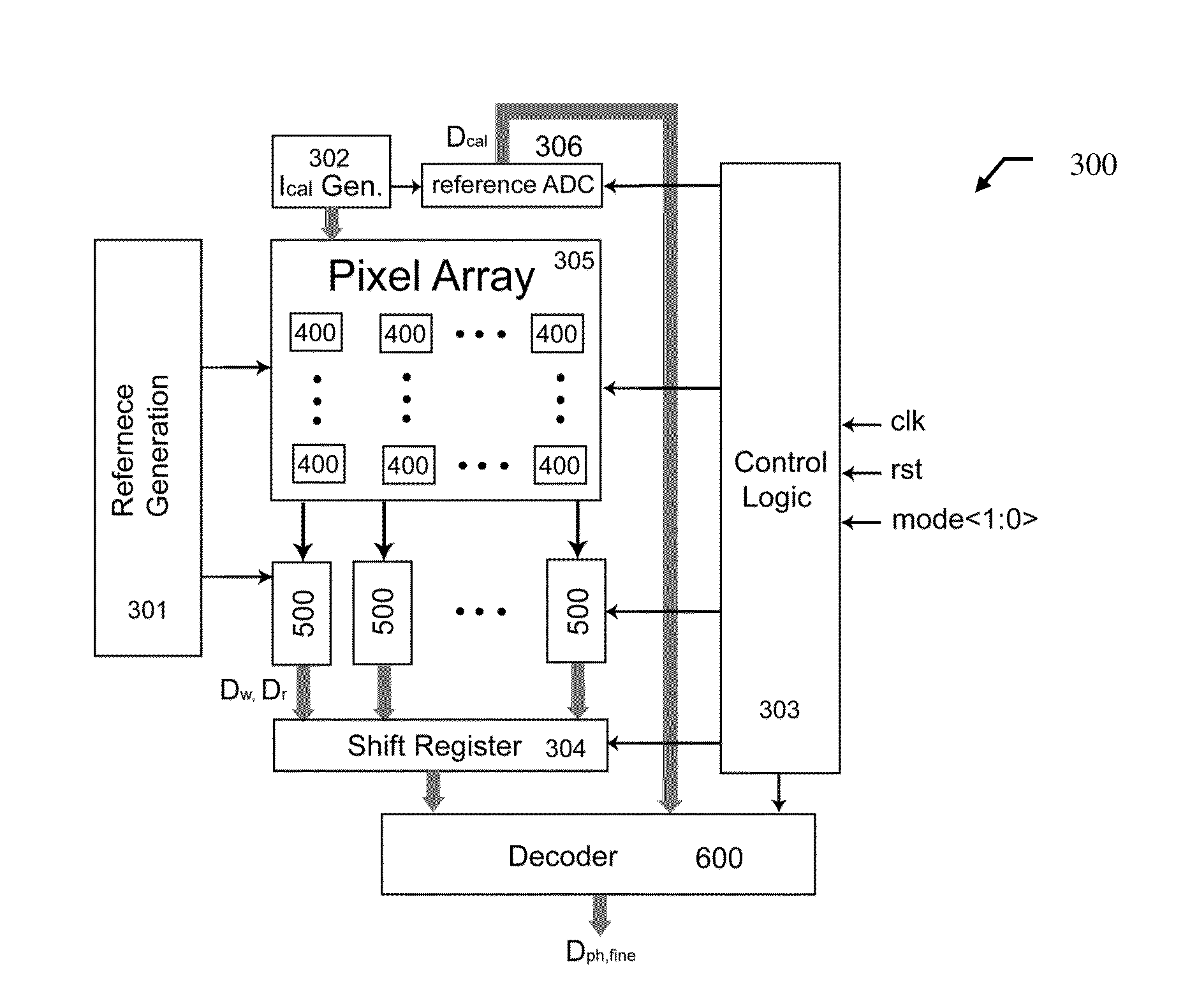
WDR Pixel Design

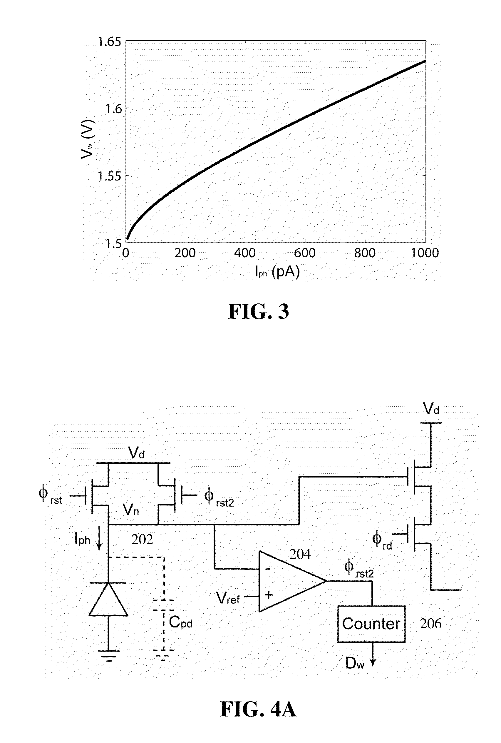
[0053]The dynamic range (DR) of a pixel is limited by the well capacity as specified by

DR=VwCint / TintImin,(1)

where Imin is the minimum photo current that the sensor can detect. This is determined by the least significant bit (LSB) size of the quantizer or the pixel read-out noise level, whichever is larger. The maximum SNR of this pixel is

SNR=Vw2qVwCint+σrd2,(2)

where σrd2 is the input-referred read-out voltage noise power.

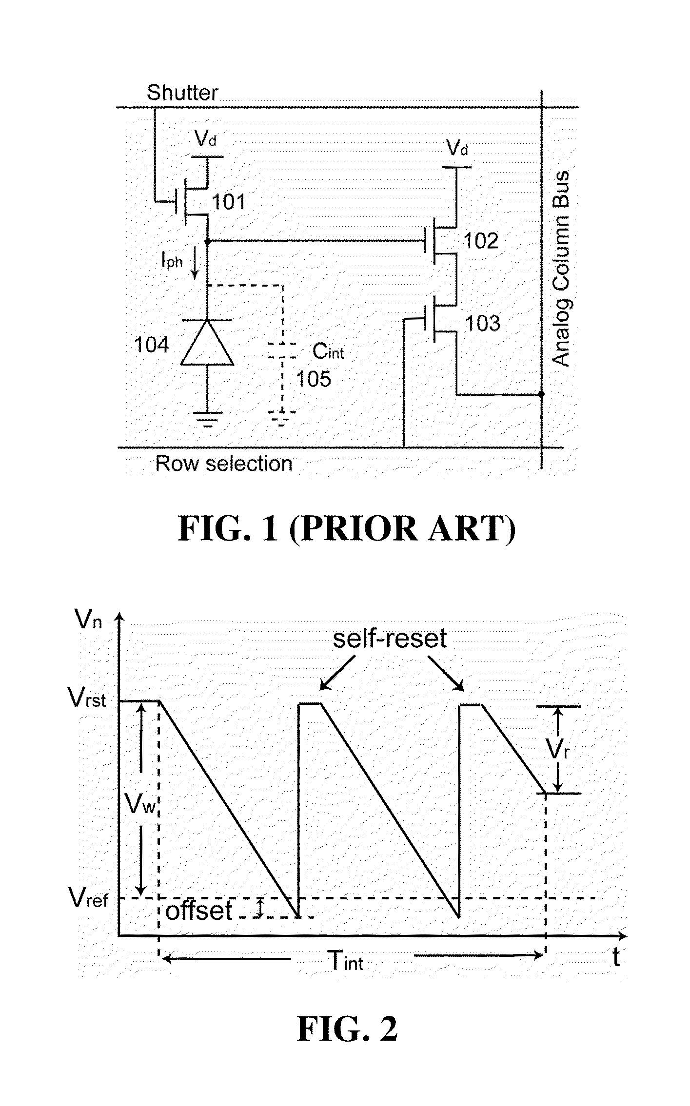
[0054]In order to design a highly linear WDR imaging sensor with high SNR, the dynamic range (DR) should be expanded linearly. In one embodiment, the DR is linearly expanded by adding a comparator 204 and a counter 206 into the pixel circuit as shown in FIG. 4A. The photo diode gets reset whenever Vn falls below the threshold voltage, as shown in FIG. 2. The number of pixel overflow events (Dw) is recorded by the counter 206. The equivalent well size in this pixel is Vrst−Vref. At the end of the accumulation, the accumulated photo voltage can be sim...


PUM


Abstract

Described herein is a circuit and related method for improving the dynamic range and the linearity characteristic of a CMOS image sensor. In various embodiments of the CMOS image sensor, a current sampler, a comparator, and a 1-bit memory are incorporated in each pixel circuit. In the image sensor, pixels are arranged in columns and a column slice is used to read the digital and analog singles from each column. In addition, a calibration circuit is incorporated in the sensor circuit for providing calibration current, which is used to generate calibration parameter. The image sensor operates in three non-overlapping modes: the difference mode, the WDR mode, and the calibration mode. The image sensor is switched among the three modes by control signals, which are provided to the image sensor by various control circuits. The image sensor normally operates in the difference mode and switches to the WDR mode when the difference between consecutive frames is over a threshold. The calibration mode allows the image sensor generate calibration parameters which are used to improve the linearity of the sensor through a interpolation method.

Description

CROSS REFERENCE TO RELATED APPLICATION[0001]This patent application claims the benefit of U.S. Provisional Patent Application No. 61 / 202,196, filed Feb. 5, 2009, which is incorporated by reference in its entirety.TECHNICAL FIELD[0002]The present invention relates in general to semiconductor image sensing and in particular to a new CMOS image sensing architecture with calibration and activity detection to achieve wide dynamic range, large signal-to-noise ratio, high linearity, low fixed-pattern noise, high fill factor, and low output data rate.BACKGROUND OF THE INVENTIONDefinition of Terms[0003]Fill factor: the fill factor of a CMOS image sensor indicates the size of the light sensitive photodiode relative to the surface of the pixel.Introduction[0004]The continuous improvement of complementary metal-oxide-semiconductor (CMOS) imaging sensors in recent years has opened up new application areas in scientific research and bio-medical diagnostics, such as space telescope, DNA microarray...

Claims


Application Information

Patent Timeline
Patent Type & Authority Applications(United States)
IPC IPC(8): H04N5/335
CPCH04N5/35527H04N5/37455H04N5/3658H04N5/365H04N25/575H04N25/67H04N25/677H04N25/772
Inventor YUAN, JIECHAN, HO YEUNG
Owner THE HONG KONG UNIV OF SCI & TECH
Why Eureka
Try Eureka