Apparatus and method for calibration of supply modulation in transmitter

a technology of supply modulation and apparatus, which is applied in the direction of gated amplifiers, duplex signal operation, baseband system details, etc., can solve the problems of large parasitic capacitance, deterioration of bandwidth, and difficulty in maintaining the phase margin characteristic of linear amplifying stages. achieve the effect of improving the stability, frequency characteristic and linearity of a hybrid supply modulator

Active Publication Date: 2013-04-18
SAMSUNG ELECTRONICS CO LTD
View PDF8 Cites 84 Cited by
  • Summary
  • Abstract
  • Description
  • Claims
  • Application Information

AI Technical Summary

Benefits of technology

[0028]Aspects of the present invention are to address at least the above-mentioned problems and / or disadvantages and to provide at least the advantages described below. Accordingly, an aspect of the present invention is to provide an apparatus and method for calibration enabling the improvement of the stability, frequency characteristic, and linearity of a hybrid supply modulator in a power amplifier.
[0031]Yet another aspect of the present invention is to provide a hybrid supply modulator capable of having a stable and wide operation band through a calibration technique of a linear amplifying stage.
[0036]In exemplary embodiments of the present invention, the supply modulator is a hybrid supply modulator, the hybrid supply modulator comprises a linear amplifying stage for receiving an envelope signal from a modulator / demodulator (modem) and for eliminating a ripple component comprised in an output signal of a switching amplifying stage and the switching amplifying stage for generating a signal for driving an RF power amplifier based on inputting of an output signal of the linear amplifying stage.
[0040]In exemplary embodiments of the present invention, the supply modulator is a hybrid supply modulator, the hybrid supply modulator comprises a linear amplifying stage for receiving an envelope signal from the modem and for eliminating a ripple component comprised in an output signal of a switching amplifying stage and the switching amplifying stage for generating a signal for driving an RF power amplifier based on inputting of an output signal of the linear amplifying stage.

Problems solved by technology

However, the maximum level of the push-pull output stage causes a big parasitic capacitance, deteriorating a BandWidth (BW) characteristic of the linear amplifying stage.
As the output load resistance value is varied, it is difficult to sufficiently maintain a phase margin characteristic of the linear amplifying stage that is designed for a specific load resistance value.
That is, a high load resistance value causes a shift of the second pole (ωp2) to a low frequency domain, causing a deterioration of the phase margin characteristic of the linear amplifying stage.
Therefore, at low RF input signal operation, the hybrid supply modulator is placed in an oscillation or unstable state.
Accordingly, a parasitic capacitance of a high-level transistor used in the push-pull output stage used for supplying large currents to the RF power amplifier 205 results in the shift of the second pole (ωp2) to the low frequency domain, causing the failure of the linear amplifying stage to have a sufficiently high GBW.
Therefore, because a ripple existing at a high frequency is not compensated by the linear amplifying stage, it deteriorates the spectrum characteristic of an output stage of the hybrid supply modulator.
However, the class-AB bias is vulnerable to a characteristic of Process Voltage Temperature (PVT) variation that is the characteristic of the RF power amplifier.

Method used


Image

  • Apparatus and method for calibration of supply modulation in transmitter
  • Apparatus and method for calibration of supply modulation in transmitter
  • Apparatus and method for calibration of supply modulation in transmitter

Examples


Embodiment Construction

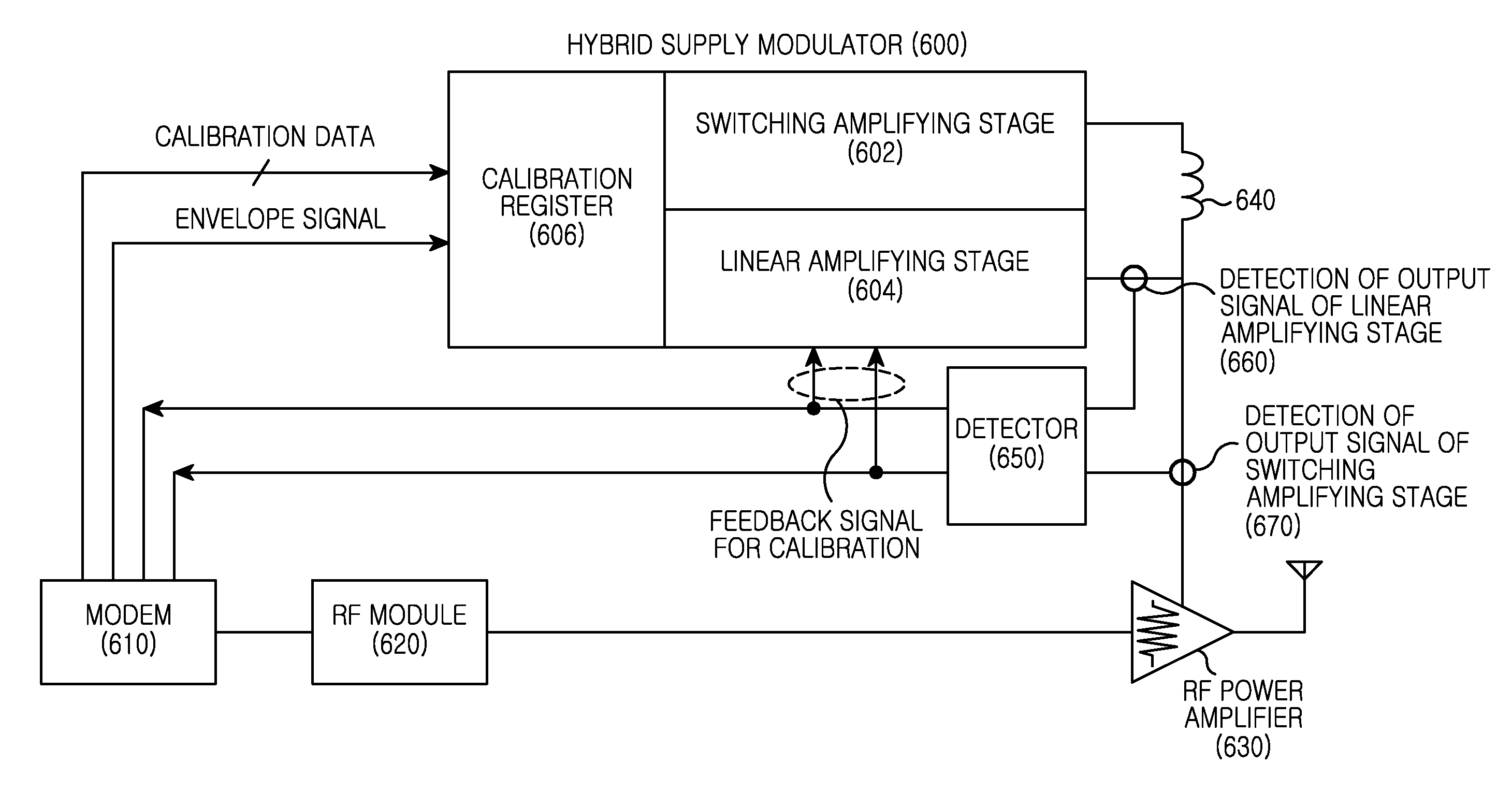
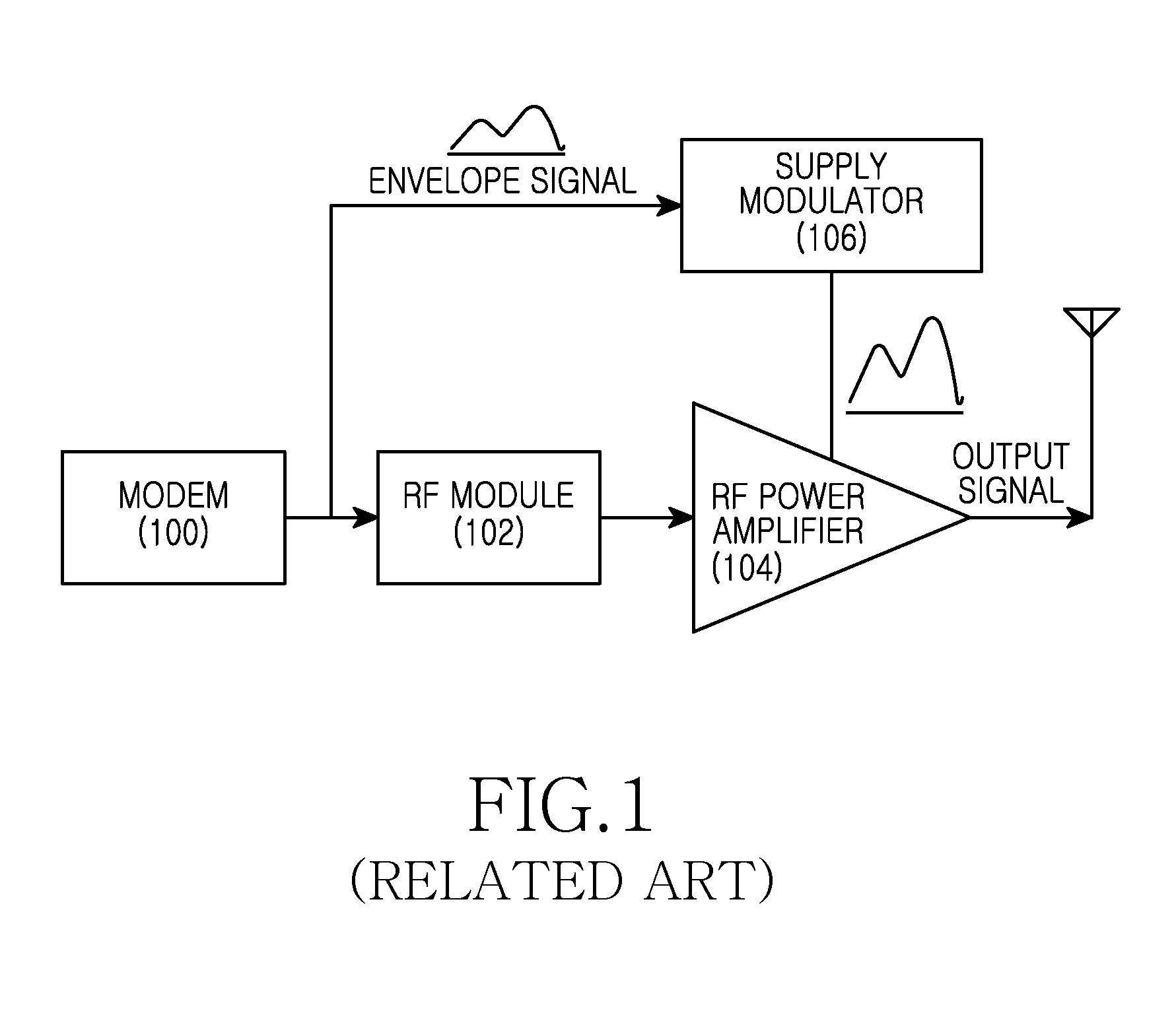
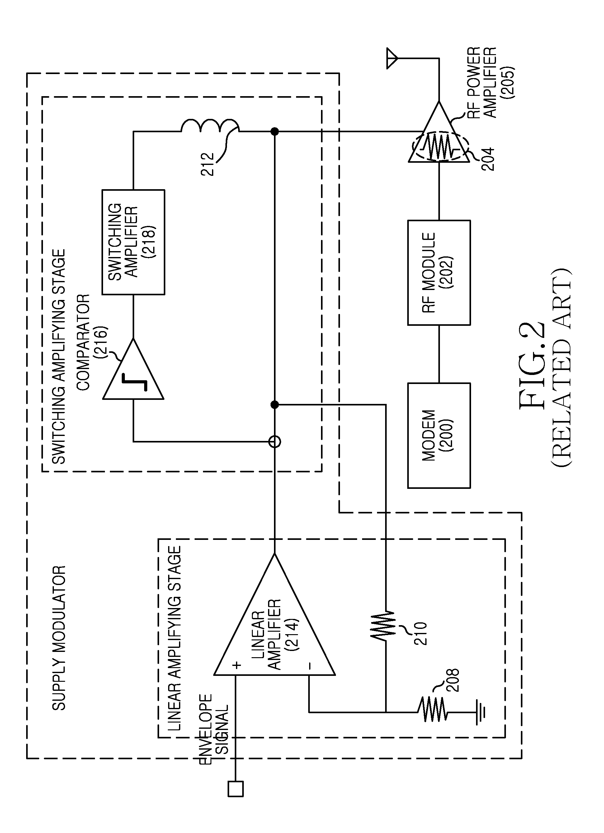
[0074]The following description with reference to the accompanying drawings is provided to assist in a comprehensive understanding of exemplary embodiments of the invention as defined by the claims and their equivalents. It includes various specific details to assist in that understanding but these are to be regarded as merely exemplary. Accordingly, those of ordinary skill in the art will recognize that various changes and modifications of the embodiments described herein can be made without departing from the scope and spirit of the invention. In addition, descriptions of well-known functions and constructions may be omitted for clarity and conciseness.

[0075]The terms and words used in the following description and claims are not limited to the bibliographical meanings, but, are merely used by the inventor to enable a clear and consistent understanding of the invention. Accordingly, it should be apparent to those skilled in the art that the following description of exemplary embod...


PUM


Abstract

A transmit apparatus having a supply modulator is provided. The apparatus includes a detector and the supply modulator. In the method, the detector detects an output signal of the supply modulator. Also, the supply modulator receives the detected output signal of the supply modulator from the detector and calibrates a modulation characteristic of the supply modulator. The transmit apparatus having a supply modulator includes a modulator / demodulator (modem) and the supply modulator. The modem provides a calibration signal for calibrating a modulation characteristic of the supply modulator, to the supply modulator. The supply modulator outputs a modulated signal in accordance with the calibrated modulation characteristic of the supply modulator based on the calibration signal from the modem.

Description

PRIORITY[0001]This application claims the benefit under 35 U.S.C. §119(a) to a Korean patent application filed on Oct. 14, 2011 in the Korean Intellectual Property Office and assigned Serial No. 10-2011-0105567, the entire disclosure of which is hereby incorporated by reference.BACKGROUND OF THE INVENTION[0002]1. Field of the Invention[0003]The present invention relates to a power amplifier of a radio transmitter. More particularly, the present invention relates to a technology of calibrating the characteristic of a linear amplifying stage of a hybrid supply modulator that modulates a supply voltage of a power amplifier of a radio transmitter.[0004]2. Description of the Related Art[0005]For the sake of long battery use time for a wireless mobile communication terminal a power management integrated circuit and a method for efficiency enhancement of a wireless power amplifier is desired. In a Wireless Broadband (WiBro) system and a Long Term Evolution (LTE) system, a wireless mobile c...

Claims


Application Information

Patent Timeline
Patent Type & Authority Applications(United States)
IPC IPC(8): H04L25/49H04B1/38
CPCH03F1/32H03F1/0222H03F2200/432H03F3/245H03F3/217H03F1/0277H03F3/193H03F3/211H03F3/3022H03F3/45475H03F3/72H03F2200/405H03F2200/462H03F2200/78H03F2203/45528H02M1/0045H03F3/24
Inventor PAEK, JI-SEONNOH, HEE-SANGLIM, HYUNG-SUNKIM, DONG-KIYANG, JUN-SEOK
Owner SAMSUNG ELECTRONICS CO LTD
Why Eureka
Try Eureka