Field effect transistor structure comprising a stack of vertically separated channel nanowires

a field effect transistor and nanowire technology, applied in the field of transistor structures, can solve the problems of high linearity, high cost, and large footprint, and achieve the effect of high linearity

Active Publication Date: 2014-12-04
THE BOARD OF TRUSTEES OF THE UNIV OF ILLINOIS
View PDF2 Cites 98 Cited by
  • Summary
  • Abstract
  • Description
  • Claims
  • Application Information

AI Technical Summary

Benefits of technology

[0005]Described herein is a field effect transistor structure that may allow high linearity to be achieved at low power and at room temperature for RF applications. A method of making such transistor structures is also described.

Problems solved by technology

Unfortunately, nonlinearity tends to be an inherent property of conventional transistors because of mobility degradation at high fields, as well as bias-dependent source / drain (S / D) resistance and channel length modulation (CLM) effect.
In addition, high linearity is extremely difficult to achieve for low power application and at room temperature.
There are many reports of linearity improvements at the circuit level by integrating and individually addressing discrete devices; however, such schemes require more resources and a larger footprint.

Method used


Image

  • Field effect transistor structure comprising a stack of vertically separated channel nanowires
  • Field effect transistor structure comprising a stack of vertically separated channel nanowires
  • Field effect transistor structure comprising a stack of vertically separated channel nanowires

Examples


example 1

Single Channel Nanowire

[0044]In this example, a single channel nanowire is uniformly p-doped at a low level (5e14 cm−3) with a relatively large diameter (Dnw=30 nm). The doping level (dopant concentration) in the S / D regions is high (e.g., ns / d, 1e19 cm−3) and the doping concentration of the S / D extension is lower (next, 2e18 cm−3). The intrinsic doping-related S / D resistance is assumed to be 2 k′Ω. The nanowire channel is surrounded by a Al2O3 gate dielectric layer of 10 nm in thickness and then a gate metal with a mid-gap workfunction of 4.5 eV (e.g., WN). A moderate value of interface charge density 5e11 cm−2 eV−1 is assumed at the GaAs / Al2O3 interface based on published experimental data. All parameters and conditions used for the simulations are for room temperature operation.

[0045]FIGS. 2A and 2B show the simulated gm vs Vgs curves as a function of nominal gate length Lg and drain bias Vds, respectively. As Lg scales down from 800 to 100 nm, the gm linearity becomes worse (FIG...

example 2

Stack of Vertically Separated Channel Nanowires

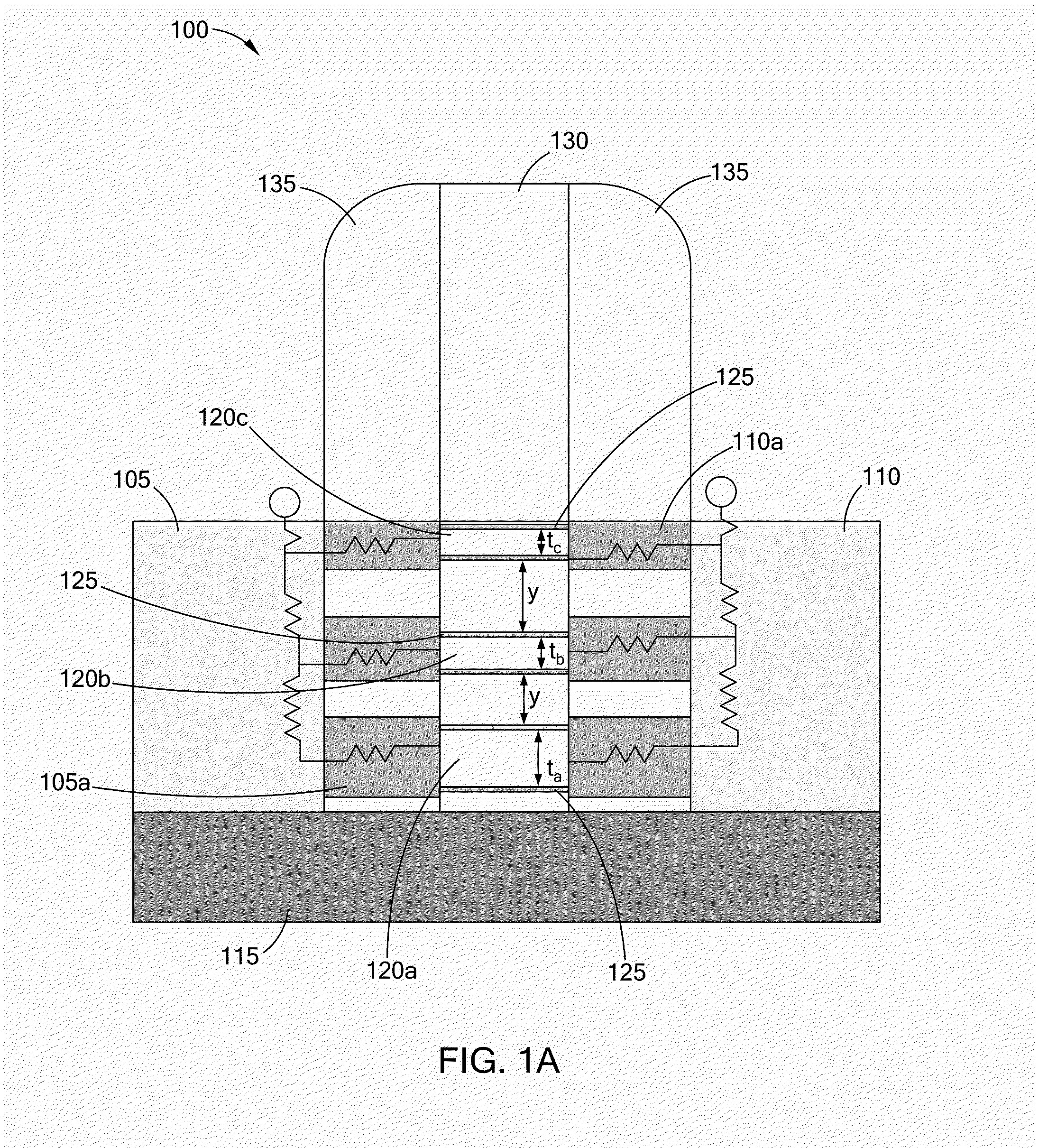
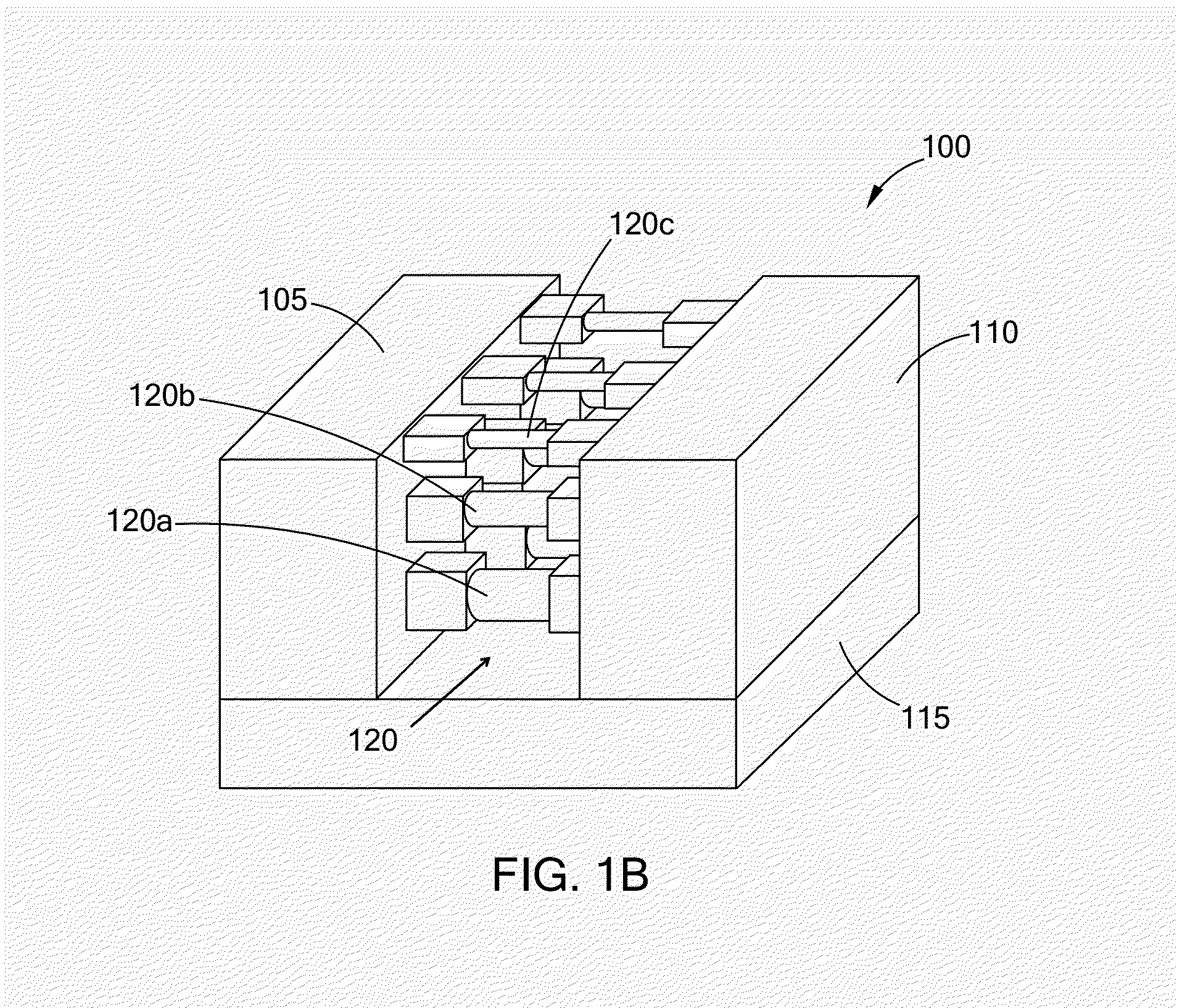
[0047]Based on the analysis of a single nanowire channel as discussed above in reference to FIGS. 2A and 2B, it is recognized that several nanowire channels with different gm versus Vgs profiles, either descending or ascending, can be superimposed within a certain range of Vgs bias to obtain a near constant total gm for the nanowire stack, and thus overall better linearity. The profile of gm versus Vgs curve can be tuned by changing the nanowire diameter (thickness) and doping concentration.

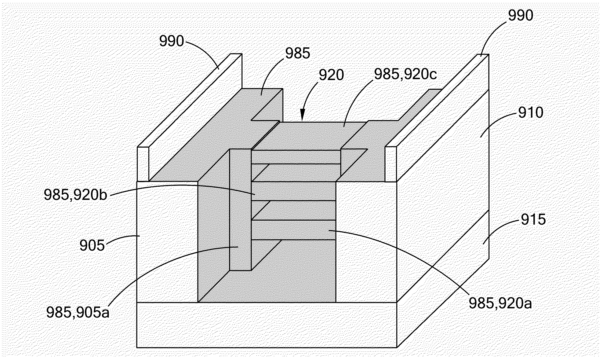
[0048]Hence, described below is a vertically stacked nanowire gate-all-around MOSFET structure that includes nanowires having different diameters (thicknesses) and doping concentrations, as illustrated in FIGS. 1A and 1B. The structure can be realized experimentally by growing epitaxially grown, lattice-matched (e.g., GaAs / AlGaAs) or strained (e.g., InGaAs / AlGaAs) layers with different thicknesses and doping concentrations on a semi-insulating substr...


PUM


Abstract

A field effect transistor structure comprises a source and a drain on a substrate, and a stack of n vertically separated channel nanowires isolated from the substrate and connecting the source and the drain, where n is an integer and 2≦n≦20. The channel nanowires collectively comprise at least two different thicknesses and/or at least two different dopant concentrations and/or at least two different semiconductor materials.

Description

RELATED APPLICATIONS[0001]This application claims priority under 35 U.S.C. §119(e) to U.S. Provisional Patent Application No. 61 / 648,246, which was filed on May 17, 2012, and which is hereby incorporated by reference in its entirety.FEDERALLY FUNDED RESEARCH OR DEVELOPMENT[0002]The invention described herein was made with government support under contract number N000141110634 awarded by the Office of Naval Research (ONR). The U.S. Government has certain rights in this invention.TECHNICAL FIELD[0003]The present disclosure is related generally to transistor structures and more particularly to field effect transistors that include stacked nanowires.BACKGROUND[0004]For transistors used for radio frequency (RF) communications, linearity is a crucial consideration for minimizing high order harmonics and intermodulation in order to achieve less distortion between input and output signals. Transistor transconductance (gm) constitutes a dominant factor for the non-linearity of RF amplifiers ...

Claims


Application Information

Patent Timeline
Patent Type & Authority Applications(United States)
IPC IPC(8): H01L29/06H01L29/66H01L29/205H01L29/78H01L29/10H01L29/20
CPCH01L29/0673H01L29/1054H01L29/20H01L29/785H01L29/205H01L29/7841H01L29/66795H01L29/2003H01L29/42392H01L29/7869
Inventor LI, XIULINGSONG, YI
Owner THE BOARD OF TRUSTEES OF THE UNIV OF ILLINOIS
Why Eureka
Try Eureka