High-voltage high-current control circuit applied to high-voltage power MOSFET (metal-oxide-semiconductor field effect transistor) circuit

A technology for controlling circuits and large currents, applied in control/regulation systems, adjusting electrical variables, instruments, etc., can solve the problems of high power MOSFET drain withstand voltage, reducing the accuracy of MOS tube current mirroring, and large voltage variation range

Active Publication Date: 2014-03-19
JIAXING ZHONGRUN MICROELECTRONICS
View PDF5 Cites 5 Cited by
  • Summary
  • Abstract
  • Description
  • Claims
  • Application Information

AI Technical Summary

Problems solved by technology

[0008] However, with the wide application of high-voltage power MOSFETs, the current setting in high-voltage power MOSFETs has become a new problem in DMOS process design
On the one hand, with the improvement of the process, the channel length of the power MOSFET is shorter, resulting in a more serious channel length modulation effect
On the other hand, the drain voltage of the power MOSFET tube is high, and the voltage variation range is large, which further reduces the current mirroring accuracy of the MOS tube.
The existing current mirror structure is no longer widely applicable to the current control of power MOSFETs under high voltage conditions

Method used


Image

  • High-voltage high-current control circuit applied to high-voltage power MOSFET (metal-oxide-semiconductor field effect transistor) circuit
  • High-voltage high-current control circuit applied to high-voltage power MOSFET (metal-oxide-semiconductor field effect transistor) circuit
  • High-voltage high-current control circuit applied to high-voltage power MOSFET (metal-oxide-semiconductor field effect transistor) circuit

Examples


Embodiment Construction

[0026] Below in conjunction with accompanying drawing, the embodiment of the present invention is described in detail: present embodiment implements under the premise of the technical scheme of the present invention, has provided detailed implementation and specific operation process, but protection scope of the present invention is not limited to the following the embodiment.

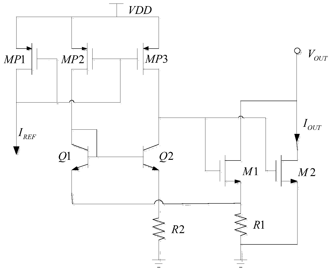
[0027] A circuit diagram of a high-current control circuit used in a high-voltage power MOSFET of the present invention is specifically as follows figure 2 As shown, it includes MOSFET tube M1, MOSFET tube M2, PMOS tube MP1, PMOS tube MP2, PMOS tube MP3, resistor R1, resistor R2, transistor Q1 and transistor Q2.

[0028] The source of the PMOS transistor MP1, the source of the PMOS transistor MP2 and the source of the PMOS transistor MP3 are connected to the power supply VDD; the gate of the PMOS transistor MP3, the gate of the PMOS transistor MP2, the gate of the PMOS transistor MP1 and the gate of t...


PUM


Abstract

A high-voltage high-current control circuit applied to a high-voltage power MOSFET (metal-oxide-semiconductor field effect transistor) circuit comprises a PMOS (P-channel metal oxide semiconductor) tube MP1, a PMOS tube MP2, a PMOS tube MP3, a triode Q1, a triode Q2, an MOSFET tube M1, an MOSFET tube M2, a resistor R1 and a resistor R2, wherein the MP1, the MP2 and the MP3 share a grid electrode; the source electrodes of the MP1, the MP2 and the MP3 are connected with a VDD; the drain electrodes of the MP2 and the MP3 are connected with the collector electrodes of the Q1 and the Q2 respectively; the base electrodes of the Q1 and the Q2 are connected with each other; the emitting electrodes of the Q1 and the Q2 are connected with the R1 and the R2 respectively; the M1 and the M2 share a grid electrode and share a drain electrode; the source electrode of the M1 is connected with the R1; the source electrode of the M2, the R1 and the R2 are grounded; the Q1 is matched with the Q2; the R1 and the R2 are resistors matched with each other according to a proportional relation; the width-to-length ratio of the M1 is proportional to that of the M2. The high-voltage high-current control circuit does not consider a channel length modulation effect of a transistor, introduces a negative feedback by the R1 and converts high current into a current comparison signal, thus achieving precise control over the current in a high-voltage high-current mode.

Description

technical field [0001] The invention relates to a current control circuit for a high-voltage power MOSFET, in particular to a high-voltage and high-current control circuit for accurately setting the current reference of an ordinary MOS tube and converting it into a high-voltage power MOSFET circuit. Background technique [0002] figure 1 is a known current source mirror circuit that mirrors the reference current I ref It is generated by the current reference source of the low temperature coefficient module, that is, BIAS, MP1 and MP2 are ordinary PMOS transistors, and MN1 and MN2 are ordinary NMOS transistors. The drain current I flowing through the NMOS transistor MN1 D1 and the drain current I flowing through the NMOS transistor MN2 D2 They are: [0003] I D 1 = 1 2 u n c ox W ...

Claims


Application Information

Patent Timeline
Patent Type & Authority Applications(China)
IPC IPC(8): G05F1/56
Inventor 朱铁柱王良坤张明星夏存宝陈路鹏黄武康殷明
Owner JIAXING ZHONGRUN MICROELECTRONICS
Why Eureka
Try Eureka