
Method for improving appearance of phosphosilicate glass by virtue of high-density plasma chemical vapor deposition (HDP CVD)

A chemical vapor deposition, phosphosilicate glass technology, applied in electrical components, semiconductor/solid-state device manufacturing, circuits, etc., can solve the problems of decreased SAC etching rate, inability to etch through contact holes, and increased bombardment intensity. Secondary sputtering, conducive to self-aligned contact hole etching, and the effect of reducing width

Active Publication Date: 2012-07-11
SHANGHAI HUAHONG GRACE SEMICON MFG CORP
View PDF0 Cites 4 Cited by
  • Summary
  • Abstract
  • Description
  • Claims
  • Application Information

AI Technical Summary

Problems solved by technology

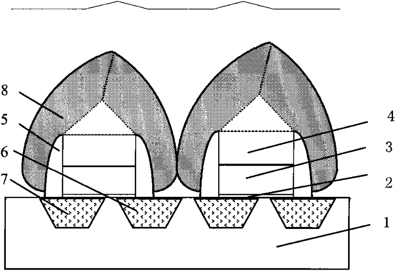
Usually, when HDP technology is used to fill high aspect ratio and small-sized channel structures (below 0.25 microns), in order to avoid voids during the hole filling process, high-power RF bias is required to increase the etching rate of plasma physical bombardment To obtain higher etching ability, thereby improving hole filling performance, but at the same time, high RF bias increases the bombardment intensity, which will also lead to aggravation of secondary sputtering, which also increases the width of the flower pattern, such as figure 1 shown
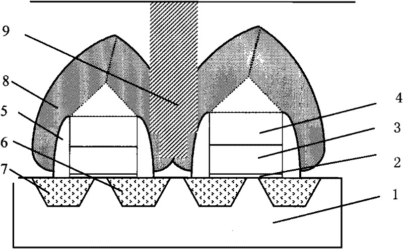
Due to the low P content in the flower pattern, the SAC etching rate decreases. If the flower pattern is too large, it will cause the etching stop phenomenon, and the contact hole 9 cannot be etched through, such as figure 2 shown

Method used


Image

  • Method for improving appearance of phosphosilicate glass by virtue of high-density plasma chemical vapor deposition (HDP CVD)
  • Method for improving appearance of phosphosilicate glass by virtue of high-density plasma chemical vapor deposition (HDP CVD)
  • Method for improving appearance of phosphosilicate glass by virtue of high-density plasma chemical vapor deposition (HDP CVD)

Examples


Embodiment Construction

[0026] The present invention will be described in further detail below in conjunction with the accompanying drawings and embodiments.

[0027] Such as Figure 3-Figure 7 As shown in the present invention, a high-density plasma chemical vapor deposition phosphosilicate glass morphology method specifically includes the following steps:

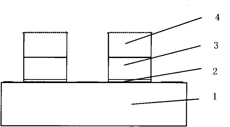
[0028] The first step is to form a gate electrode on the silicon substrate 1, using a conventional process method, generally first depositing a gate oxide layer 2 on the silicon substrate 1, then depositing a polysilicon layer 3 on the gate oxide layer 2, and then Depositing a silicon nitride layer 4 on the polysilicon layer 3, polysilicon photolithography and etching, forming a polysilicon gate electrode, see image 3 ;

[0029] In the second step, LDD (Light Doped Drain, lightly doped source and drain regions) is implanted, and then sidewalls 5 are formed on the sidewalls of the gate electrode. The sidewalls 5 are formed by using a conventio...


PUM


Abstract

The invention discloses a method for improving the appearance of phosphosilicate glass by virtue of high-density plasma chemical vapor deposition (HDP CVD), comprising the following steps: (1) forming a gate electrode on a silicon substrate; (2) carrying out LDD (laser detector diode) injection and forming a side wall at the side wall of the gate electrode; (3) carrying out drain and source injection and fast thermal annealing; (4) adopting an HDP CVD process to deposit a phosphosilicate glass film, and introducing etching gas to react with the phosphosilicate glass in the process; and (5) carrying out self-aligned contact hole etching. In the method, the etching gas is introduced in the traditional HDP CVD process, so that the etching capability is improved, non-hole filling is guaranteed to be realized under a low-power radio-frequency bias voltage, and simultaneously, secondary sputtering in the deposition process is reduced, therefore, the width of a shell (flow pattern) with low P content formed on the surface of the phosphosilicate glass due to secondary sputtering is reduced, the appearance of the phosphosilicate glass film is improved, and the method is more beneficial to self-aligned contact hole etching.

Description

technical field [0001] The invention belongs to the field of semiconductor integrated circuit manufacturing, in particular to a high-density plasma chemical vapor deposition (HDP CVD) method, in particular to a method for improving the morphology of phosphosilicate glass deposited by high-density plasma chemical vapor deposition. Background technique [0002] Sub-atmospheric pressure chemical vapor deposition borophosphosilicate glass film (SACVD BPSG) is widely used before metal deposition as the insulating layer PMD (pre-metal dielectric) between the metal layer and the underlying polysilicon. Among them, P can absorb alkaline ions, and B can lower the glass transition temperature of the BPSG film, so that it can be reflowed and planarized at a lower temperature. However, as the feature size continues to decrease, the hole filling performance of SACVD BPSG cannot meet the requirements, that is, voids will appear during the hole filling process, which will cause a short cir...

Claims


Application Information

Patent Timeline
Patent Type & Authority Patents(China)
IPC IPC(8): H01L21/316H01L21/336
Inventor 彭仕敏谢烜
Owner SHANGHAI HUAHONG GRACE SEMICON MFG CORP
Learn More