Method for manufacturing printed circuit board (PCB)

A circuit board manufacturing and circuit board technology, which is applied in the fields of printed circuit manufacturing, printed circuit, and removal of conductive materials by chemical/electrolytic methods, which can solve the problem of difficult recycling of copper foil waste and high cost of circuit board manufacturing, etc. problem, achieve high industrial utilization value, reduce the time required for etching, and reduce the effect of manufacturing cost

Inactive Publication Date: 2011-06-01
INVENTEC CORP
View PDF0 Cites 4 Cited by
  • Summary
  • Abstract
  • Description
  • Claims
  • Application Information

AI Technical Summary

Problems solved by technology

[0003] Because in the process of etching the copper foil, a large amount of etching solution needs to be used to etch the part of the copper foil that is not wired. Generally speaking, there is usually a large area on the copper foil that needs to be etched away. Therefore, it is necessary to use a large amount of etching solution to achieve the desired etching effect, and the copper foil waste is usually dissolved in the etching solution during the etching process, and the copper foil waste dissolved in the etching solution is difficult to recycle, so Causes the manufacturing cost of the circuit board to remain high

Method used


Image

  • Method for manufacturing printed circuit board (PCB)
  • Method for manufacturing printed circuit board (PCB)
  • Method for manufacturing printed circuit board (PCB)

Examples


Embodiment Construction

[0020] Embodiments of the present invention are described below through specific examples, and those skilled in the art can easily understand other advantages and effects of the present invention from the content disclosed in this specification. The present invention can also be implemented or applied through other different specific examples, and various modifications and changes can be made to the details in this specification based on different viewpoints and applications without departing from the spirit of the present invention.

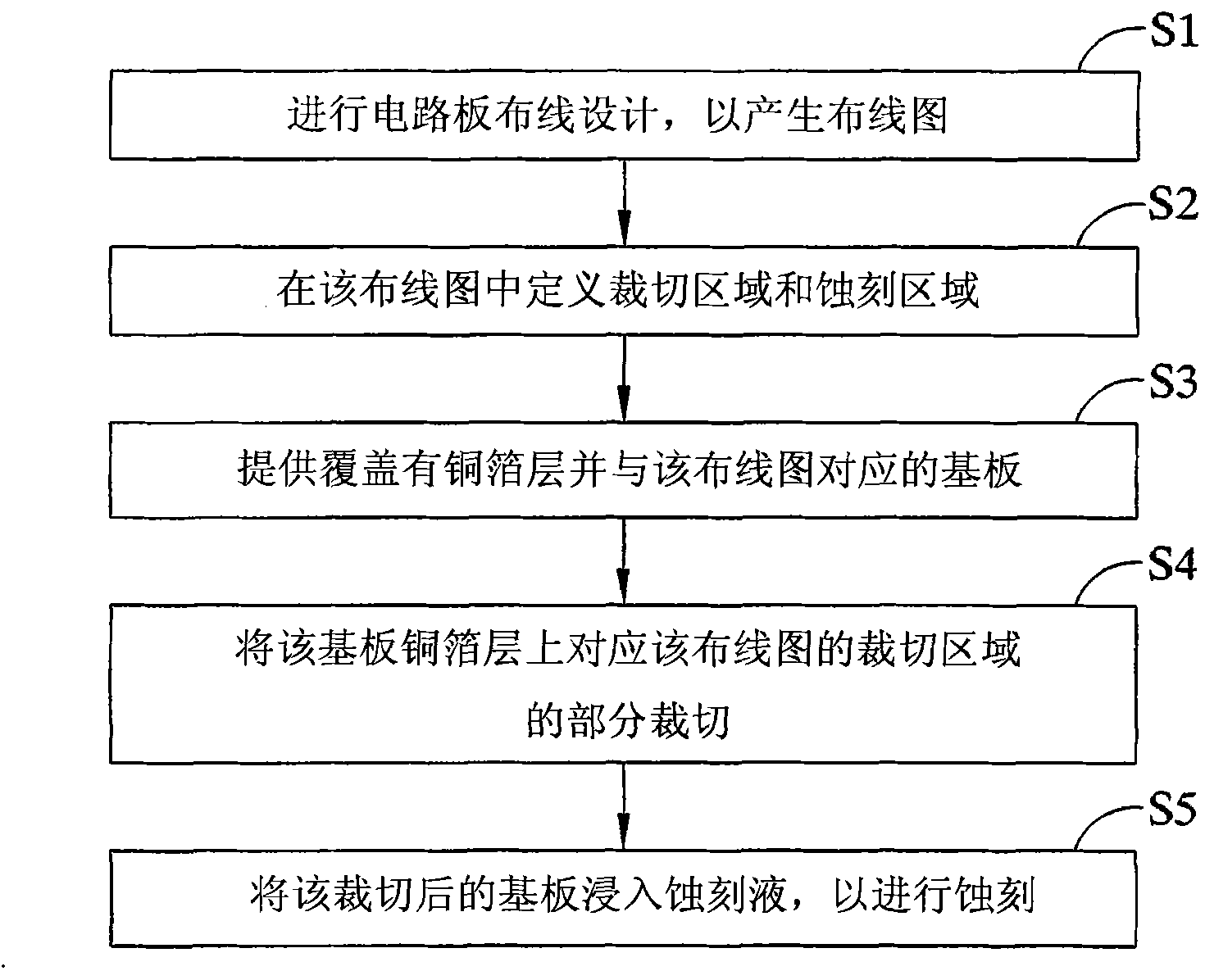
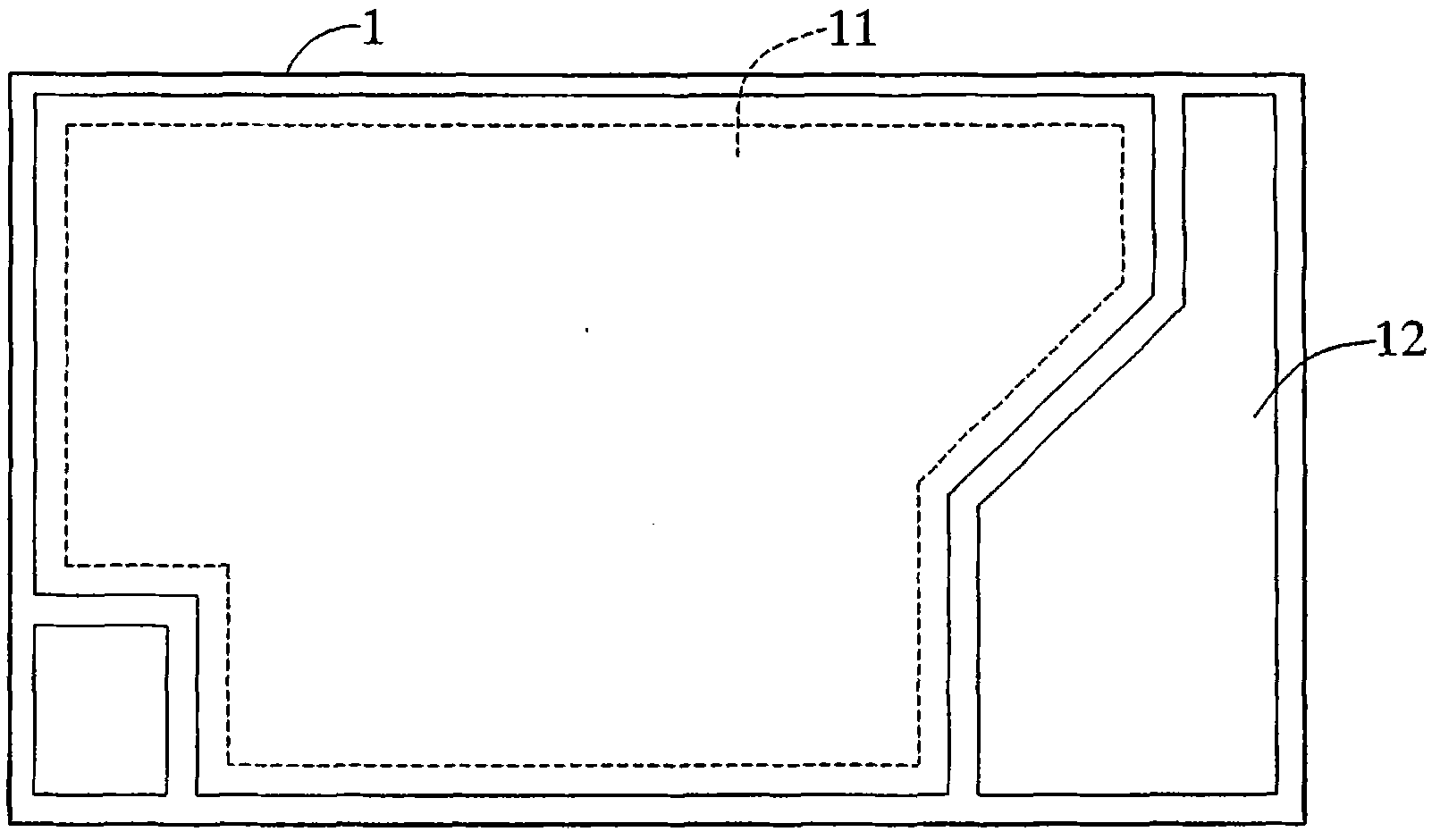
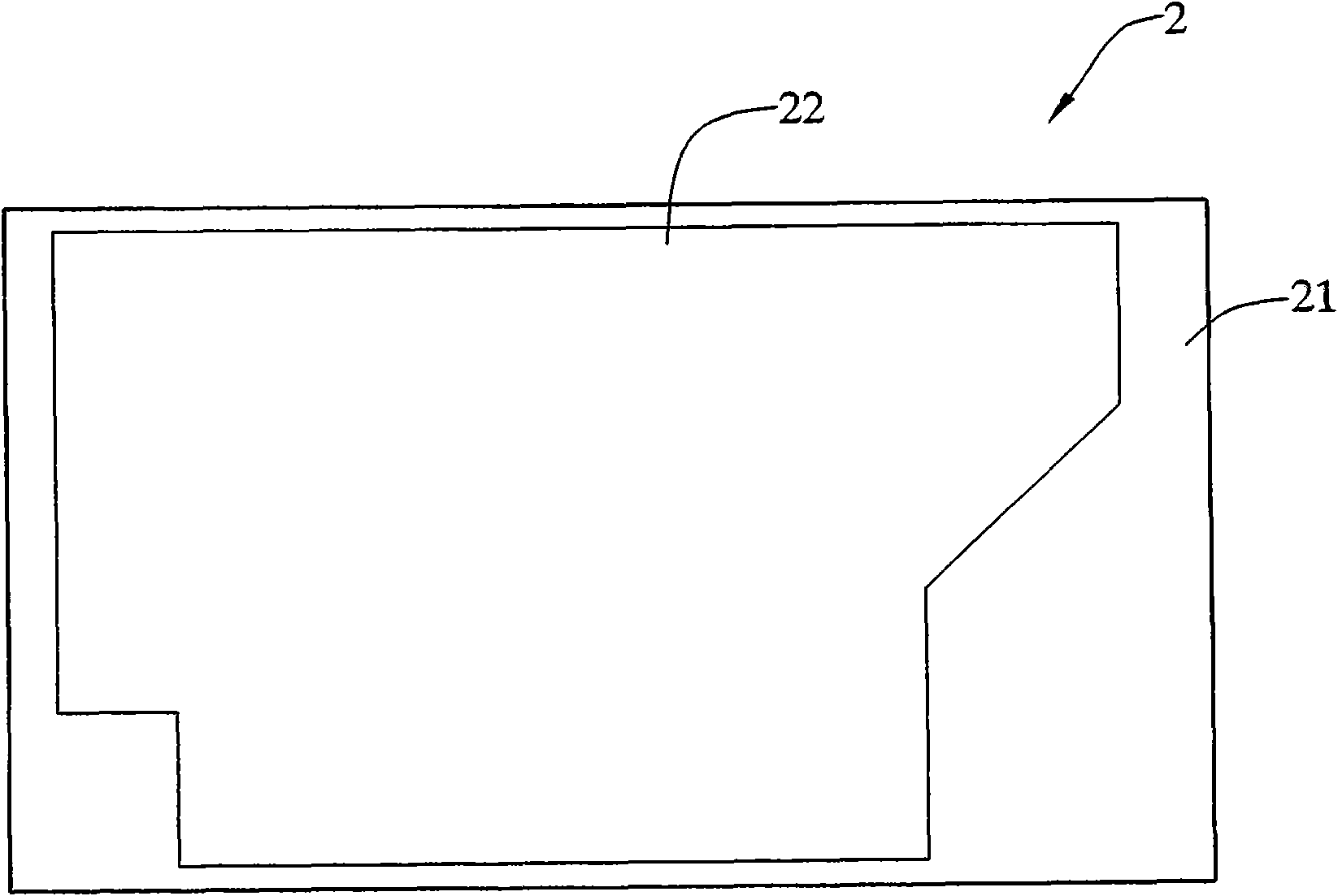
[0021] see figure 1 , figure 2 and image 3 ,in, figure 1 It is a flow chart illustrating the steps of the circuit board manufacturing method of the present invention; figure 2 A schematic diagram illustrating a circuit template produced by the circuit board manufacturing method of the present invention; and image 3 It is a schematic diagram showing a substrate covered with cut copper foil produced by the circuit board manufacturing metho...


PUM


Abstract

The invention provides a method for manufacturing a printed circuit board (PCB). The method comprises the following steps: firstly carrying out PCB wiring design to generate a wiring pattern; defining a cropping area and an etching area in the wiring pattern; then providing a substrate corresponding to the wiring pattern, wherein the substrate is covered by a copper foil layer; cropping the part corresponding to the cropping area in the wiring pattern, of the copper foil layer on the substrate; and finally soaking the cropped substrate into an etchant for etching, and forming a wiring circuit on the copper foil layer on the substrate, so the method has the following beneficial effects: the copper foil layer part dispensing with wiring, on the substrate can be cropped before etching so as to reduce the usage amount of the etchant for etching the copper foils and the time required for etching and conduce to recycling the waste copper foils, thus reducing the environmental pollution caused by manufacturing the PCB and achieving the effects of lowering the manufacturing cost, and the like.

Description

technical field [0001] The invention relates to a method for manufacturing a circuit board, in particular to a method for manufacturing a circuit board that can save manufacturing costs. Background technique [0002] The structure of the printed circuit board mainly includes a metal layer substrate and a coverlay covering the metal layer substrate. In the metal layer substrate structure, copper foil is mainly used as the material. In the manufacturing process of the circuit board, the copper foil with the same size as the metal layer substrate is usually covered on the substrate, and then solid copper is added on the copper foil. (thieving pad) to uniformly etch out the wiring lines, and then etch away the copper foil on the circuit board that is not part of the wiring lines, so as to retain the part of the copper foil that needs to be laid out later. This part is used to provide circuits. Circuit connections for parts on the board. [0003] Because in the process of etchi...

Claims


Application Information

Patent Timeline
Patent Type & Authority Applications(China)
IPC IPC(8): H05K3/00H05K3/06
Inventor 金新国范文纲
Owner INVENTEC CORP
Why Eureka
Try Eureka