Thin film transistor substrate and liquid crystal display panel
A technology of liquid crystal display panels and thin film transistors, applied in static indicators, nonlinear optics, optics, etc., can solve the problems of decreased transmittance, poor liquid crystal efficiency, difficult balance, etc., achieve low color shift technology, improve color Offset phenomenon, reducing the effect of too long boundaries between bright and dark areas
- Summary
- Abstract
- Description
- Claims
- Application Information
AI Technical Summary
Problems solved by technology
Method used
Image

Examples
no. 1 example
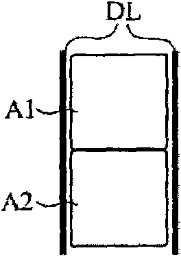
[0045] Figure 2A It is a schematic diagram of wiring of a single pixel region P of a thin film transistor substrate 1 of a liquid crystal display panel according to the first embodiment of the present invention, Figure 2B for Figure 2A An enlarged schematic view of region A in . Wherein, the liquid crystal display panel may further include a color filter substrate (not shown in the figure) and a liquid crystal material layer (not shown in the figure), and the liquid crystal material layer is interposed between the two substrates.
[0046] The thin film transistor substrate 1 includes a substrate 11, a plurality of data lines D N and D N+1 , a plurality of scanning lines (not shown in the figure) and a plurality of pixel electrodes 12 . Wherein, the substrate 11 is a glass substrate, and the plurality of data lines and the plurality of scanning lines are interlacedly arranged on the substrate 11, and the plurality of data lines and the plurality of scanning lines define ...
no. 2 example
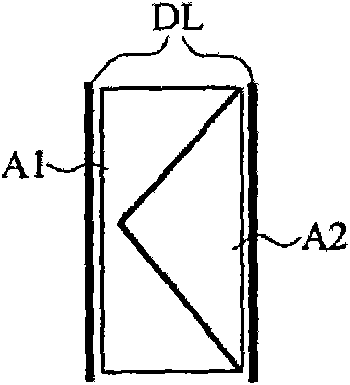
[0055] Figure 4A and Figure 4B A liquid crystal display panel according to a second embodiment of the present invention is shown. The liquid crystal display panel includes a first substrate 2 , a second substrate 3 and a liquid crystal material layer (not shown) sandwiched between the first substrate 2 and the second substrate 3 . in, Figure 4A The first substrate 2 is shown, and the first substrate 2 is an example of a thin film transistor substrate; Figure 4B The second substrate 3 is shown, and the second substrate 3 is a color filter substrate as an example.
[0056] Such as Figure 4A As shown, multiple data lines D N 、D N+1 with multiple scan lines S M , S M+1 Intersecting on the first substrate 2 , the data lines and the scan lines can define a plurality of pixel regions P. Figure 4A It is a schematic wiring diagram of a single pixel region P.
[0057] A plurality of pixel electrodes 22 are disposed in the plurality of pixel regions P correspondingly. In...
no. 3 example
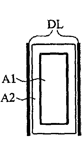
[0063] Figure 6A and Figure 6B A liquid crystal display panel according to a third embodiment of the present invention is shown. The liquid crystal display panel includes a first substrate 4 , a second substrate 5 and a liquid crystal material layer (not shown) sandwiched between the first substrate 4 and the second substrate 5 . in, Figure 6A The first substrate 4 is shown, and the first substrate 4 is a thin film transistor substrate as an example; Figure 6B The second substrate 5 is shown, and the second substrate 5 is a color filter substrate as an example.
[0064] Such as Figure 6A As shown, multiple data lines D N 、D N+1 with multiple scan lines S M , S M+1 Intersecting on the first substrate 4 , the data lines and the scan lines can define a plurality of pixel regions P. Figure 6A It is a schematic wiring diagram of a single pixel region P.
[0065] A plurality of pixel electrodes 42 are disposed in the plurality of pixel regions P correspondingly. The...
PUM
 Abstract
Description
Claims
Application Information
 - Generate Ideas
- Intellectual Property
- Life Sciences
- Materials
- Tech Scout
- Unparalleled Data Quality
- Higher Quality Content
- 60% Fewer Hallucinations
Browse by: Latest US Patents, China's latest patents, Technical Efficacy Thesaurus, Application Domain, Technology Topic, Popular Technical Reports.
© 2025 PatSnap. All rights reserved.Legal|Privacy policy|Modern Slavery Act Transparency Statement|Sitemap|About US| Contact US: help@patsnap.com