

Manufacture method of capacitive touch screen
A technology of capacitive touch screen and conductive layer is applied in the direction of electrical digital data processing, input/output process of data processing, instruments, etc., which can solve the problems of high cost, low efficiency, complicated production steps, etc., so as to reduce the production process and save the process. Time, effect of reducing material cost and equipment investment
Inactive Publication Date: 2011-06-15
安徽晟光科技有限公司
View PDF3 Cites 19 Cited by
- Summary
- Abstract
- Description
- Claims
- Application Information
AI Technical Summary
Problems solved by technology
The purpose of the present invention is to provide a method for manufacturing a capacitive touch screen aimed at the shortcomings of the existing double-sided capacitive touch screen electrode manufacturing method, such as complicated manufacturing steps, low efficiency, and high cost.
Method used
View moreImage
Smart ImageViewing Examples

Examples
Embodiment Construction
Login to View More PUM
| Property | Measurement | Unit |
|---|---|---|
| strength | aaaaa | aaaaa |
| thickness | aaaaa | aaaaa |
| thickness | aaaaa | aaaaa |
Abstract
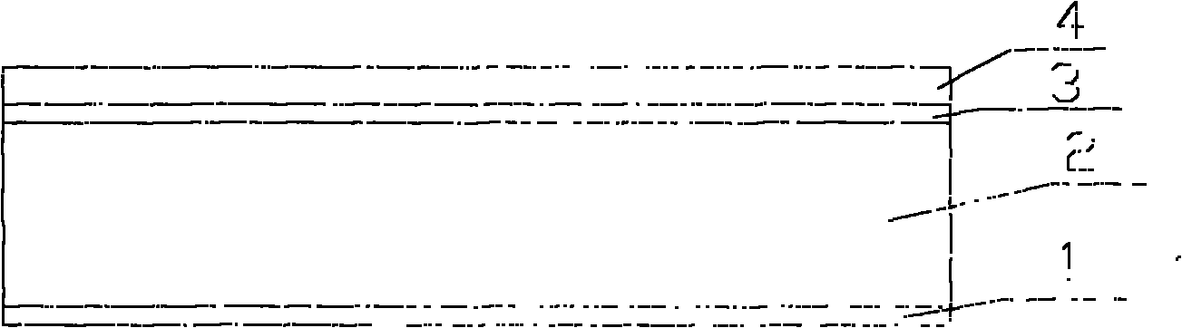
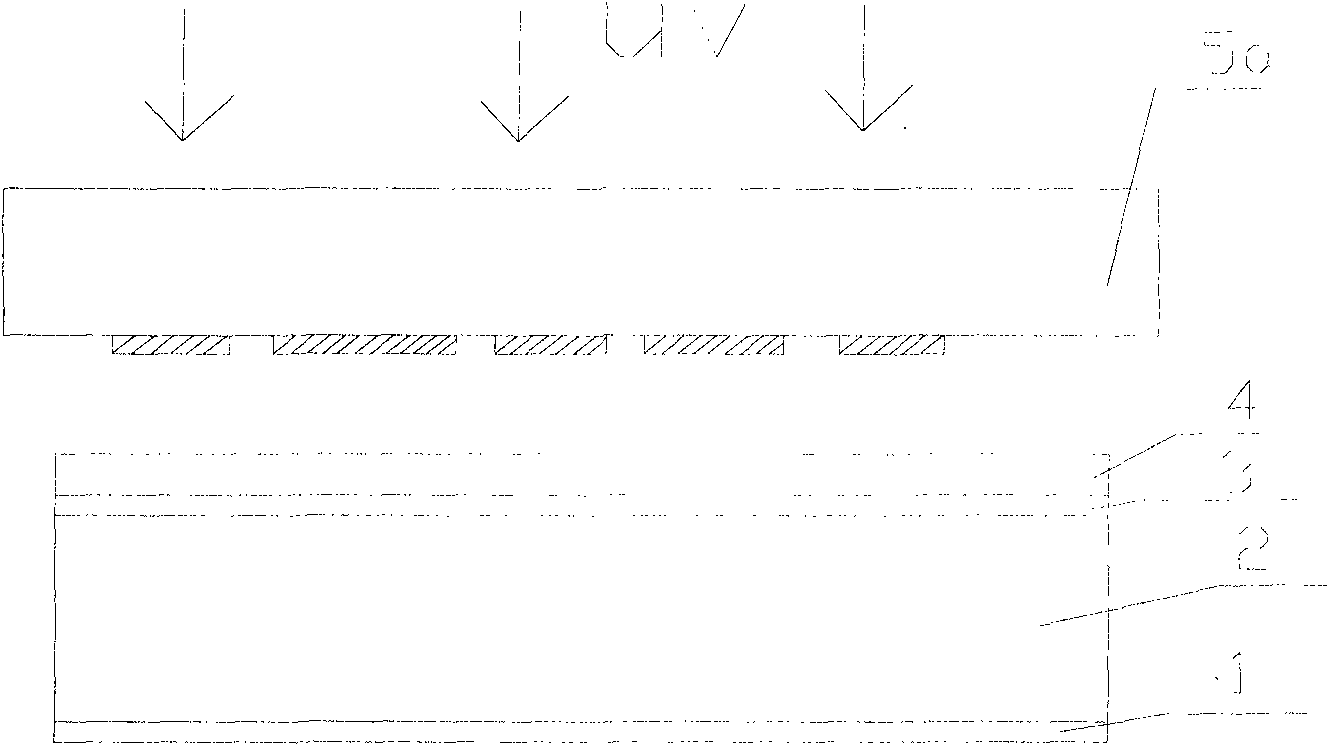
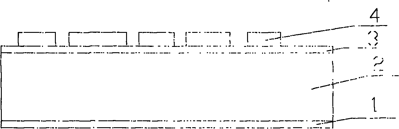
The invention relates to a manufacture method of a capacitive touch screen. The method is characterized by comprising the steps: 1. respectively plating conducting layers on the surface a and the surface b of a baseplate; 2. coating a photoresist on the surface a; 3. exposing and developing the photoresist on the surface a; 4. passivating the photoresist on the surface a: i.e. decomposing the photosensitizer of the photoresist in a heating way at an infrared tunnel furnace, wherein the heating temperature is within the range of 115- 150 DEG C, and the heating time is within the range of 120-3600 seconds; 5: coating a photoresist on the surface b; 6. exposing and developing the photoresist on the surface b; 7. hardening the photoresist coated on the surface b in a heating way, wherein the heating temperature is within the range of 100 DEG C to 150 DEG C, and the heating time is within the range of 120-3600 seconds; 8. simultaneously etching transparent conducting materials at two surfaces; and 9. removing the photoresists at the two surfaces. The method has the advantages that since the photoresist on the surface a is passivated, the photosensitizer of the photoresist on the surface a is decomposed, and the transparent conducting patterns at the two surfaces are simultaneously etched, therefore, the production process can be reduced, the flow time can be saved, the material cost can be reduced, and the equipment investment can be reduced.
Description
A method of making a capacitive touch screen technical field The invention relates to a method for manufacturing a touch screen in electronic components, in particular to a method for manufacturing a double-sided capacitive touch screen electrode. Background technique The capacitive touch screen can realize multi-point and accurate touch sensing, and has a simple structure and high light transmittance. It is the mainstream direction of the current development of display touch technology. The row electrodes and the column electrodes of the double-sided capacitive touch screen are respectively arranged on the front surface b of the substrate. The problem in the manufacturing process is: the photoresist is coated on the a side of the substrate, and after photolithography and hardening, the photoresist protective layer must be coated on the b side of the substrate to etch the conductive layer on the a side; After removing the photoresist on the front side b, apply the photore...
Claims
Login to View More Application Information
Patent Timeline
 Patent Type & AuthorityApplications(China)
IPC IPC(8): G06F3/044
Inventor周朝平关玉华肖新煌林钟权董宏碧黄赵华刘萍萍
Owner安徽晟光科技有限公司