Semiconductor device and method for manufacturing the same

A technology for semiconductors and devices, applied in the field of semiconductor devices and their manufacturing, can solve problems such as increased cost, increased number of processes, and inability to form component areas, and achieves the effect of cost reduction

Inactive Publication Date: 2011-06-15
KK TOSHIBA
View PDF6 Cites 10 Cited by
  • Summary
  • Abstract
  • Description
  • Claims
  • Application Information

AI Technical Summary

Problems solved by technology

Therefore, the structure of the element region and the structure of the terminal region cannot be formed in the same process in common, and the number of steps increases and the cost increases.

Method used


Image

  • Semiconductor device and method for manufacturing the same
  • Semiconductor device and method for manufacturing the same
  • Semiconductor device and method for manufacturing the same

Examples


Embodiment Construction

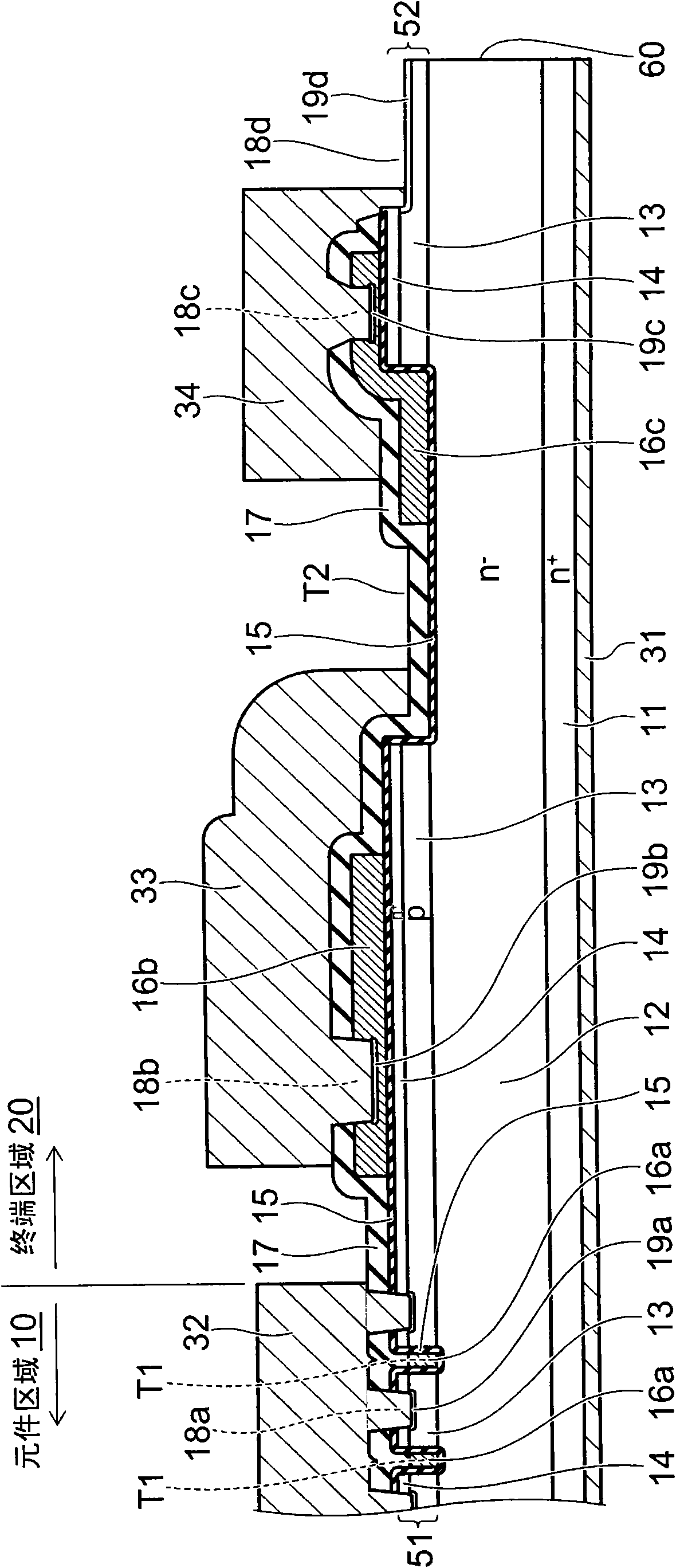
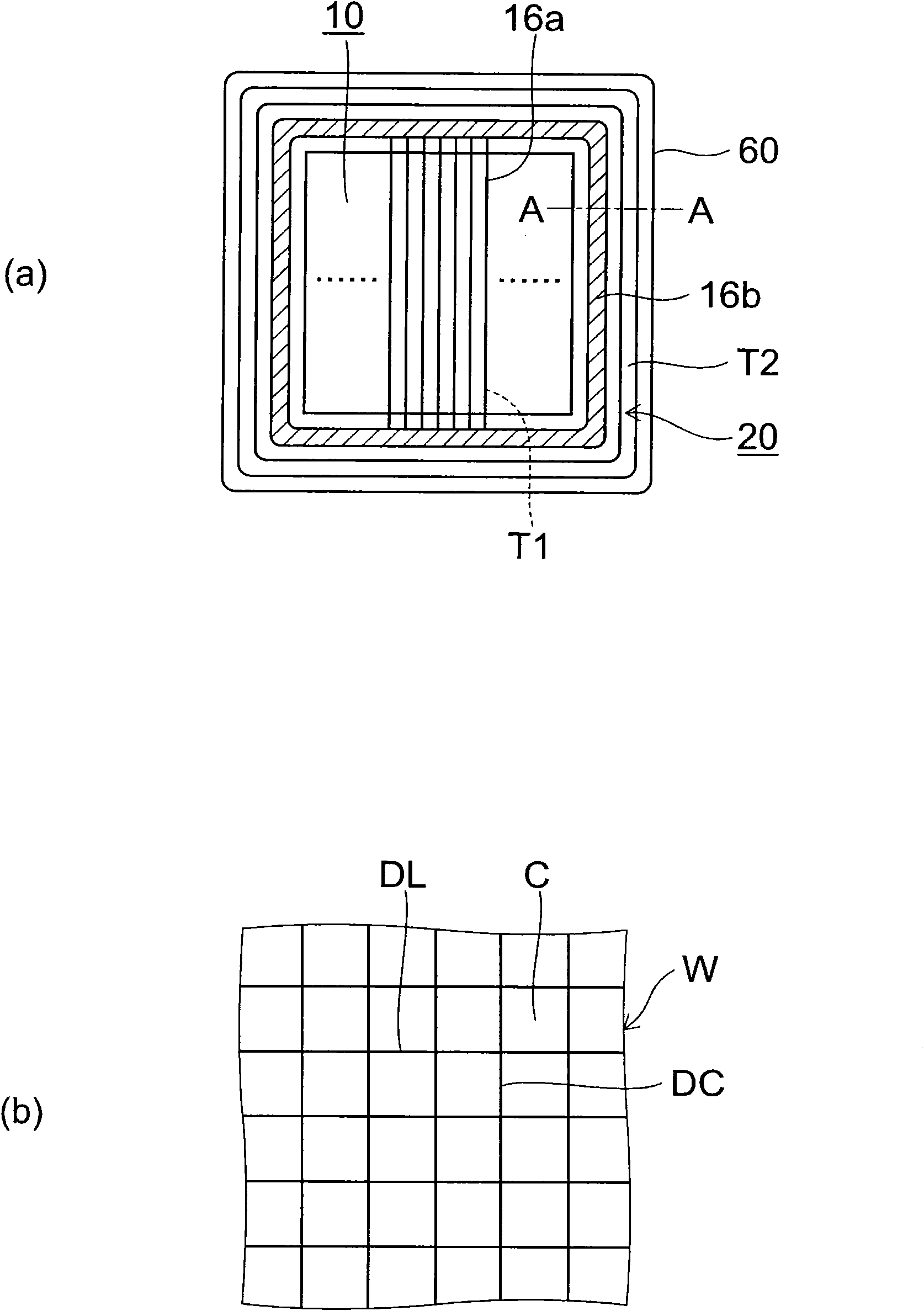
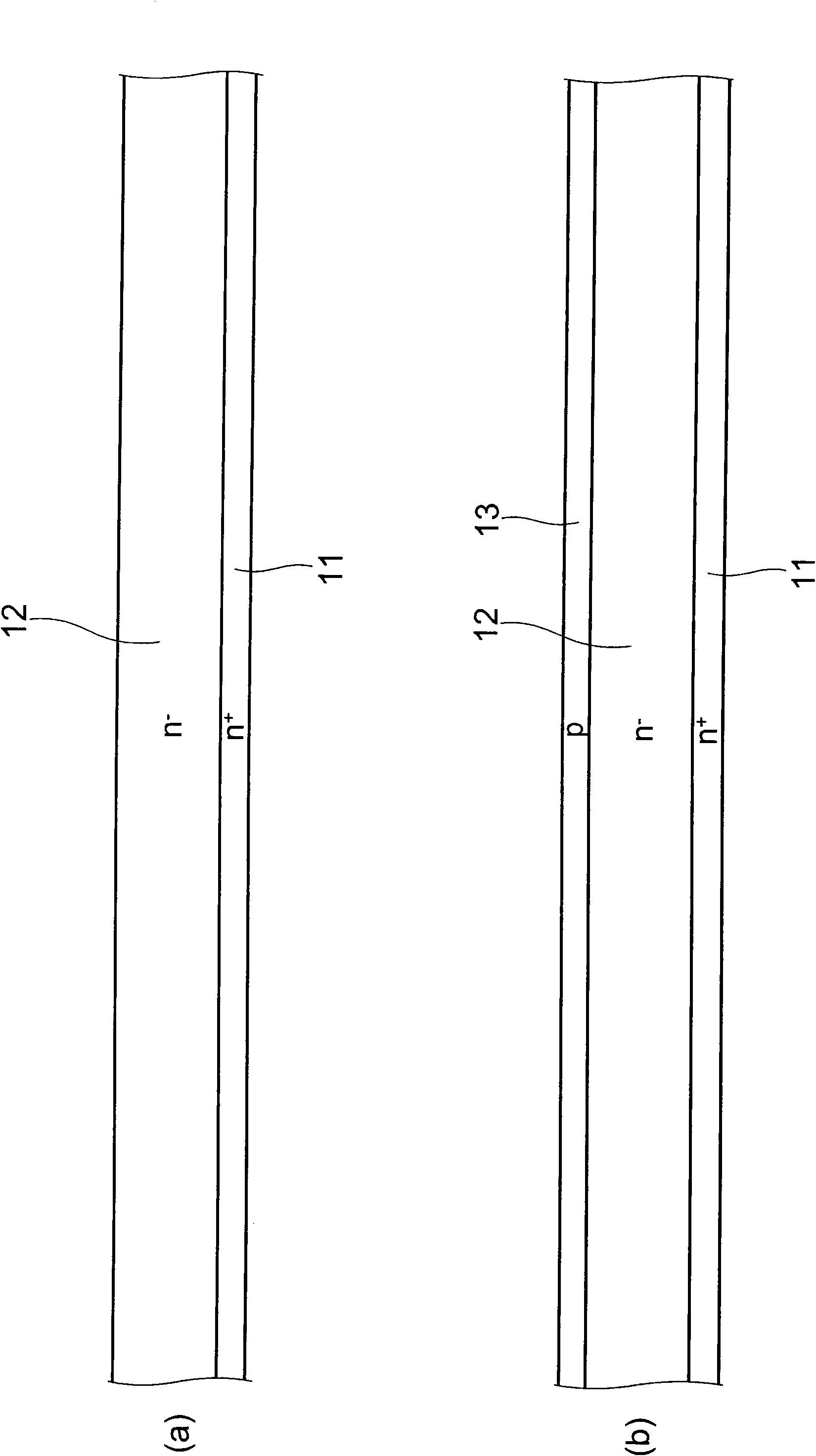
[0016] According to an embodiment, a semiconductor device includes a first semiconductor layer of the first conductivity type, a second semiconductor layer of the first conductivity type, a third semiconductor layer of the second conductivity type, a fourth semiconductor layer of the first conductivity type, a first trench A groove, a second trench, an insulating film, a gate electrode, a first main electrode, a second main electrode, a channel stopper layer, and a channel stopper electrode. The second semiconductor layer is provided on the first semiconductor layer, and has a lower first conductivity type impurity concentration than the first semiconductor layer. The third semiconductor layer is disposed on the second semiconductor layer. The fourth semiconductor layer is disposed on the third semiconductor layer, and the impurity concentration of the first conductivity type is higher than that of the second semiconductor layer. The first trench penetrates through the fourth...


PUM


Abstract

The invention provides a semiconductor device and a method for manufacturing the same. The semiconductor device comprises: a first semiconductor layer of a first conductivity type; a second semiconductor layer of the first conductivity type; a third semiconductor layer of a second conductivity type; a fourth semiconductor layer of the first conductivity type; first trenches which penetrate the fourth semiconductor layer and the third semiconductor layer to reach the second semiconductor layer; a second trench which penetrates the fourth semiconductor layer and the third semiconductor layer, on a side closer to a termination than the first trenches, to reach the second semiconductor layer, the second trench dividing the fourth semiconductor layer and the third semiconductor layer into a element part including a region wherein the first trenches are formed and a termination part; an insulating film; a gate electrode; a first main electrode; a second main electrode; a channel stopper layer provided in the second trench via the insulating film; and a channel stopper electrode provided on the termination part of the third semiconductor layer and the termination part of the fourth semiconductor layer and connecting the channel stopper layer and the termination part.

Description

[0001] This application is based on, and claims priority from, Japanese Priority Patent Application No. 2009-282526 filed on December 14, 2009, which is hereby incorporated by reference in its entirety. technical field [0002] The invention relates to a semiconductor device and a manufacturing method thereof. Background technique [0003] In power semiconductor devices, it is necessary to terminate the base and the source. For example, Japanese Patent Application Laid-Open No. 2009-505434 discloses that a source dopant is implanted using a mask in order to selectively form a source region in an element region. That is, in order to determine the source region, it is necessary to form a mask by photolithography and etching. The source region is not formed on the termination region. Therefore, the structure of the element region and the structure of the terminal region cannot be formed in the same process in common, and the number of steps increases and the cost increases. ...

Claims


Application Information

Patent Timeline
Patent Type & Authority Applications(China)
IPC IPC(8): H01L29/78H01L29/41H01L21/336H01L21/28
CPCH01L29/407H01L29/0638H01L29/41766H01L29/402H01L29/7811H01L29/42372H01L29/0696H01L29/66727H01L29/4238H01L29/66734H01L29/7813
Inventor 富田幸太松田升浦秀幸
Owner KK TOSHIBA
Why Eureka
Try Eureka