Supercharge Your Innovation With Domain-Expert AI Agents!

Semiconductor device

A semiconductor, conductive type technology, applied in semiconductor devices, semiconductor/solid-state device manufacturing, transistors, etc., can solve problems such as difficulty in increasing the integration density of EDMOS transistors

Active Publication Date: 2011-06-15
KEY FOUNDRY CO LTD
View PDF5 Cites 13 Cited by
  • Summary
  • Abstract
  • Description
  • Claims
  • Application Information

AI Technical Summary

Problems solved by technology

[0008] Because the adjacent active regions 22 are isolated from each other by the P-type impurity region 14 having a conductivity type different from that of the N-type second well 12, this conventional EDMOS transistor has the following defects: In addition to the P-type impurity region 14, a non-conductive operating region in order to ensure isolation between the active regions 22 which may have different potentials from each other and also to allow a sufficiently high operating voltage of the active region 22
[0010] The need to include non-operating regions makes it difficult to increase the integration density of EDMOS transistors
This problem may not be a problem only associated with EDMOS transistors, but may be common to all junction-isolated high-voltage semiconductor devices

Method used


Image

  • Semiconductor device
  • Semiconductor device
  • Semiconductor device

Examples


Embodiment Construction

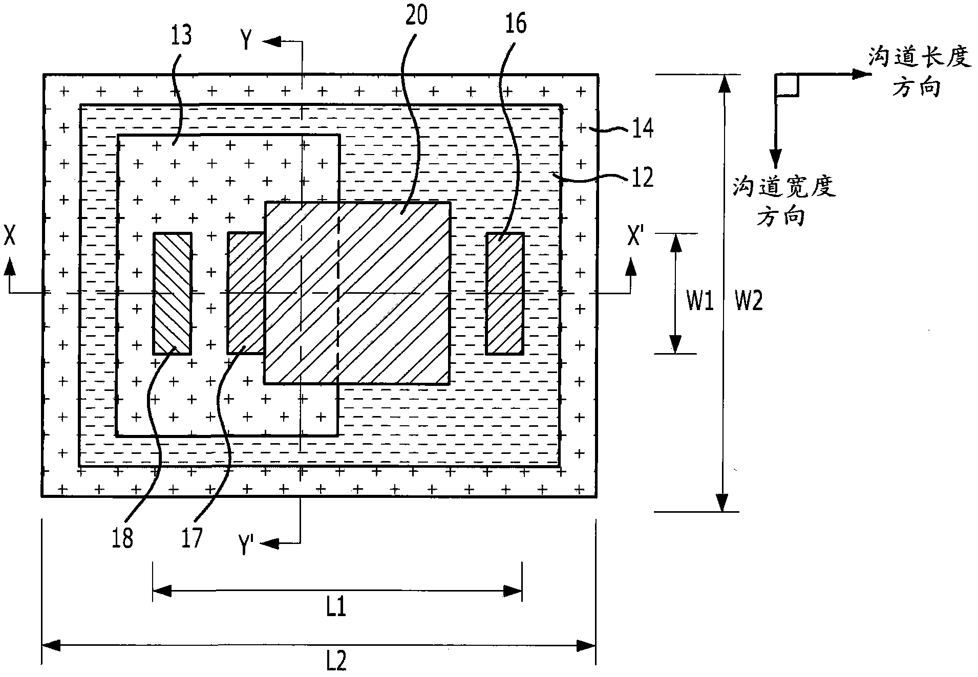
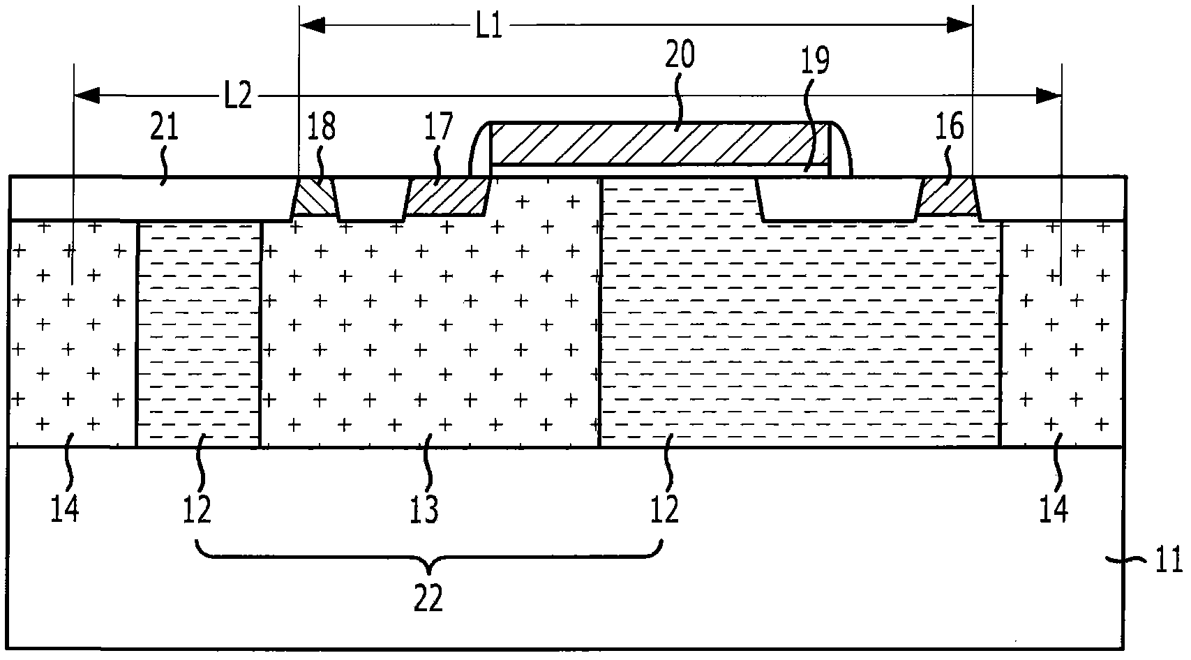
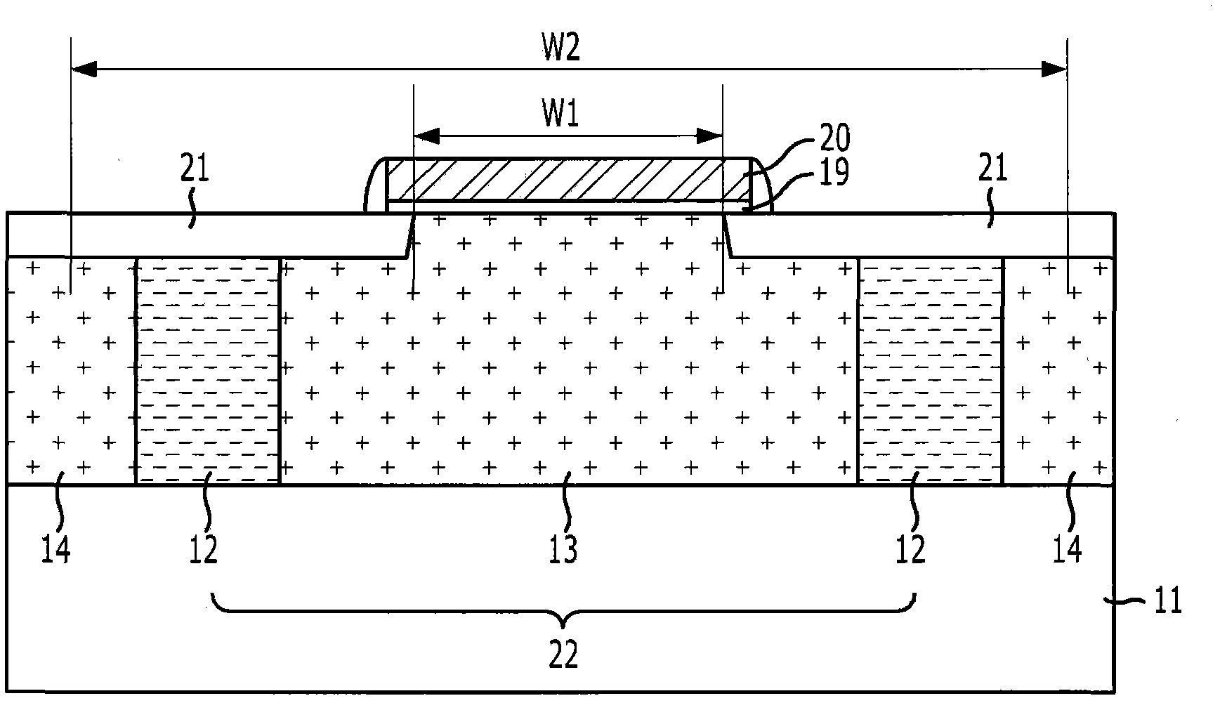
[0038] Several embodiments of the present invention will be described in detail below with reference to the accompanying drawings. It should be understood that these embodiments are not intended and should not be construed as limiting the full scope of the invention, and that aspects and features of the invention may be realized using constructions, arrangements, and components other than those specifically detailed in those embodiments described herein. accomplish. Rather, these embodiments are provided so that this disclosure will be thorough and complete, and will fully convey the scope of the invention to those skilled in the art. Throughout this disclosure, like reference numerals refer to like parts throughout the various figures and embodiments of this disclosure. The drawings are not necessarily drawn to scale and, in some instances, proportions may have been exaggerated for clarity. When a first layer is referred to as being "on" a second layer or "on" a substrate, ...


PUM


Abstract

A semiconductor device includes a substrate with one or more active regions and an isolation layer formed to surround an active region and to extend deeper into the substrate than the one or more active regions. The semiconductor further includes a gate electrode, which covers a portion of the active region, and which has one end portion thereof extending over the isolation layer.

Description

[0001] Cross References to Related Applications [0002] This application claims priority under 35 U.S.C. §119 to Korean Patent Application No. 10-2009-110927 filed on November 17, 2009, which is hereby incorporated by reference in its entirety. technical field [0003] The present invention relates generally to the fabrication of semiconductor devices; and more particularly to the fabrication of high voltage semiconductor devices. Background technique [0004] Various integrated circuits including one or more high voltage transistors together with low voltage circuitry are widely used in different electrical applications. High voltage transistors such as extended drain MOS (EDMOS) transistors, lateral double diffused MOS (LDMOS) transistors, and the like occupy a large amount of space in such integrated circuits. [0005] To keep pace with the trend towards higher integration densities, there is also a need to scale down high voltage semiconductor devices in size while sti...

Claims


Application Information

Patent Timeline
Patent Type & Authority Applications(China)
IPC IPC(8): H01L29/78H01L29/06H01L29/423H01L27/088
CPCH01L29/0653H01L29/7835H01L29/1083H01L29/4238H01L21/76264H01L29/7816H01L29/7391H01L29/42312
Inventor 车载汉李倞镐金善玖崔莹石金胄浩蔡桭荣吴仁泽
Owner KEY FOUNDRY CO LTD
Features
  • R&D
  • Intellectual Property
  • Life Sciences
  • Materials
  • Tech Scout
  • Unparalleled Data Quality
  • Higher Quality Content
  • 60% Fewer Hallucinations
Learn More