
Hermetic mems device and method for fabricating hermetic mems device and package structure of hermetic mems device

A micro-electro-mechanical system and packaging structure technology, applied in the direction of micro-structure technology, micro-structure devices, manufacturing micro-structure devices, etc., can solve the problems of production yield and high cost

Active Publication Date: 2011-06-29
SOLID STATE SYST
View PDF5 Cites 12 Cited by
  • Summary
  • Abstract
  • Description
  • Claims
  • Application Information

AI Technical Summary

Problems solved by technology

[0005] However, this conventional process has certain disadvantages, including high cost, production yield issues due to packaging three components into the device, and parasitic effects of combining MEMS with the sensing IC

Method used


Image

  • Hermetic mems device and method for fabricating hermetic mems device and package structure of hermetic mems device
  • Hermetic mems device and method for fabricating hermetic mems device and package structure of hermetic mems device
  • Hermetic mems device and method for fabricating hermetic mems device and package structure of hermetic mems device

Examples


Embodiment Construction

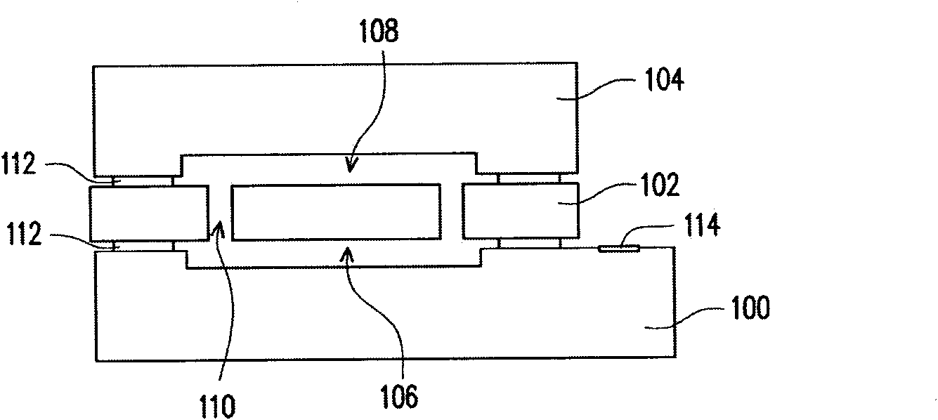
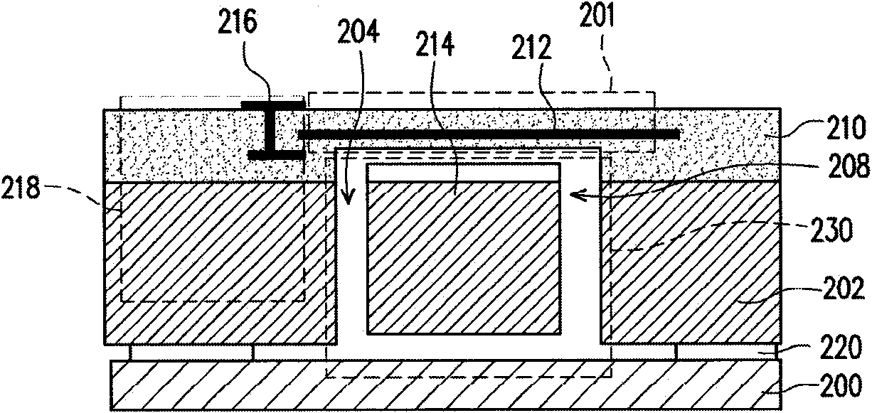
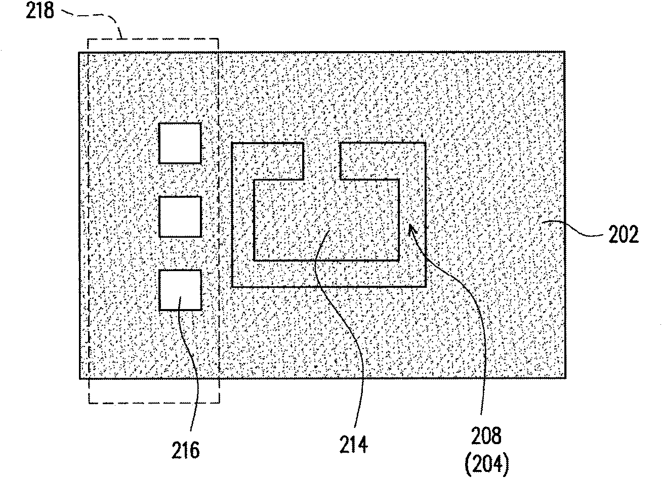
[0039] In the present disclosure, novel sealed MEMS devices in several embodiments have been proposed. The sealed MEMS package has at least the following characteristics. Integration between IC and MEMS increases high performance. The MEMS and the sensing IC are fabricated in the same substrate to avoid parasitic effects of combining the MEMS with the sensing IC. The encapsulation layer may be formed over one side of the MEMS element by an interconnect process known from CMOS technology. Chip scale package (CSP) and wafer level package (WLP) are available for small size and low cost processes. An additional substrate is attached to the other side of the MEMS using wafer-to-wafer bonding or fusion to form a hermetic package.

[0040] Several examples are provided for description. However, the present invention is not limited to the disclosure of the embodiments. In addition, the embodiments can also be appropriately combined with each other.

[0041] Figure 2A is a cros...


PUM


Abstract

The present invention provides a hermetic microelectromechanical system (MEMS) package including a CMOS MEMS chip and a second substrate. The CMOS MEMS Chip has a first substrate, a structural dielectric layer, a CMOS circuit and a MEMS structure. The structural dielectric layer is disposed on a first side of the first structural substrate. The structural dielectric layer has an interconnect structure for electrical interconnection and also has a protection structure layer. The first structural substrate has at least a hole. The hole is under the protection structure layer to form at least a chamber. The chamber is exposed to the environment in the second side of the first structural substrate. The chamber also comprises a MEMS structure. The second substrate is adhered to a second side of the first substrate over the chamber to form a hermetic space and the MEMS structure is within the space.

Description

technical field [0001] The present invention relates to a microelectromechanical system (MEMS) device. More particularly, the present invention relates to the structure and fabrication process of MEMS devices. Background technique [0002] MEMS devices have been proposed in various applications. However, MEMS devices are usually in an open environment. Since the MEMS structure of a MEMS device is sensitive to ambient air, operation in an open environment may pick up noise. Hermetically sealed packages for MEMS devices have thus been proposed. [0003] Hermetic MEMS packages have features that include isolation of the MEMS structure from the external environment. For example, damping of air and thermal noise can be avoided by creating a vacuum environment for the MEMS. Additionally, the sealed chamber can protect the MEMS device from EM interference and result in a small size MEMS device with high performance and low cost of adoption. Applications for hermetic MEMS pack...

Claims


Application Information

Patent Timeline
Patent Type & Authority Applications(China)
IPC IPC(8): B81B7/02
CPCB81B2207/07B81B2207/092B81C2203/0714B81B2207/015H01L2224/48091B81C1/00246H01L2224/48247H01L2924/1461B81B7/0064H01L2924/00014H01L2924/00
Inventor 李建兴谢聪敏刘志成
Owner SOLID STATE SYST
Learn More