Method for improving grinding efficiency of test sample of transmission electron microscope

An electron microscope, a technology for testing samples, applied in the field of semiconductor manufacturing, can solve the problems of reducing production efficiency, easily broken samples, difficult to identify samples, etc., to achieve the effect of improving grinding efficiency

Inactive Publication Date: 2011-06-29
SEMICON MFG INT (SHANGHAI) CORP
View PDF0 Cites 6 Cited by
  • Summary
  • Abstract
  • Description
  • Claims
  • Application Information

AI Technical Summary

Problems solved by technology

[0008] From the method of grinding three samples in the above-mentioned prior art, it can be seen that for three or more samples, in order to reflect the patterns of all sample TEM tests in the Cu grid aperture, one of them must be thinned or even Multiple samples, in the backside grinding process, not only takes a lot of time, but once the backside of the sample is ground very thin, the sample is easy to crack (crack), after the crack appears, the sample is difficult to identify under TEM
Although the production efficiency of the prior art method is significantly improved compared with the traditional method of grinding two samples at the same time, once a problem occurs, the production efficiency will be reduced instead.
[0009] Moreover, there is also a problem in the prior art: after grinding, when the ion milling (ion milling) makes a thin area for TEM testing, since there is only one Cu grid in the prior art, the ion beam hits the sample through the aperture of the Cu grid On the pattern, and the area inside the aperture is relatively small, so when the patterns of sample 1 and sample 2 are hit first, and then the pattern of sample 3 is hit, the patterns of sample 1 and sample 2 before ion milling have been destroyed. Cannot be preserved, continue to be used as TEM test

Method used


Image

  • Method for improving grinding efficiency of test sample of transmission electron microscope
  • Method for improving grinding efficiency of test sample of transmission electron microscope
  • Method for improving grinding efficiency of test sample of transmission electron microscope

Examples


Embodiment Construction

[0025] In order to make the object, technical solution, and advantages of the present invention clearer, the present invention will be further described in detail below with reference to the accompanying drawings and examples.
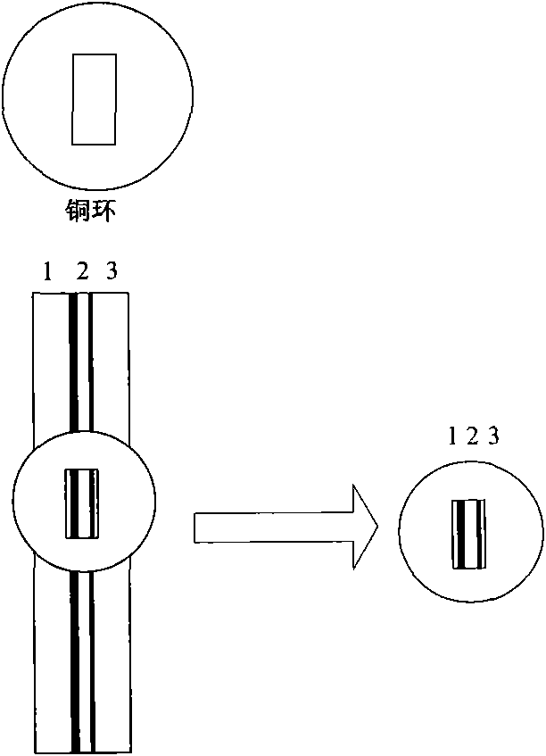
[0026] The core idea of ​​the present invention is: for more than two samples, that is, three or more TEM test samples, it is not necessary to thin the back of the samples, directly paste the samples in order, and then paste a plurality of Cu grid, so that the patterns of all sample TEM tests are reflected in the Cu grid aperture, thereby greatly improving the grinding efficiency of TEM test samples.

[0027] In the specific embodiment of the present invention, the simultaneous grinding of three samples is taken as an example for illustration.

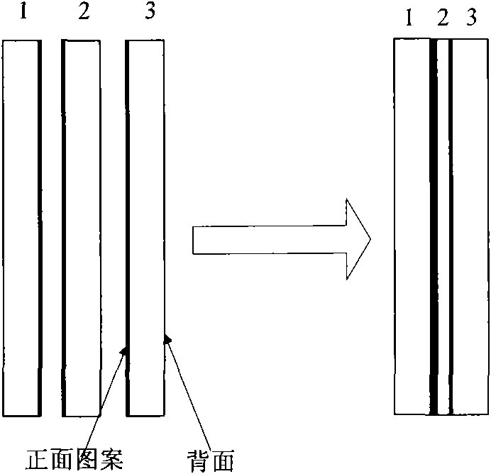
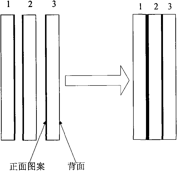
[0028] see Figure 2a , use professional glue to paste samples 1 to 3 on the front or back in order to form a whole. The sample can be any part of the chip that needs to be tested. It is a rectangular (square...


PUM


Abstract

The invention discloses a method for improving grinding efficiency of test samples of a transmission electron microscope (TEM) for grinding more than two samples simultaneously; the samples are rectangular samples with predetermined thickness, comprising a face pattern of the sample and a semiconductor substrate on the back. The method comprises the following steps that: for more than two samples, the faces or the backs are orderly integrally stuck; two opposite lateral surfaces of the integral sample are grinded to reduce the distance between two opposite lateral surfaces of the sample; after one lateral surface of the integral sample is ground and before the other lateral surface is ground, the method further comprises the following step: the target positions on the lateral surfaces of the grinded integral sample are stuck with a plurality of copper rings for embodying the pattern of each grinded sample. The method effectively improves the grinding efficiency of the test samples of the TEM.

Description

technical field [0001] The invention relates to the technical field of semiconductor manufacturing, in particular to a method for improving the grinding efficiency of a transmission electron microscope test sample. Background technique [0002] At present, in the field of semiconductor manufacturing technology, when making samples under a transmission electron microscope (TEM, Transmission Electron Microscope) for testing, an important method is to polish the samples to achieve the required test thickness requirements . [0003] In order to improve the efficiency of grinding samples in the prior art, the traditional method of grinding two samples at the same time has been improved, and three or more samples are simultaneously ground, combined with Figure 1a to Figure 1b A prior art method for milling three samples is described. [0004] see Figure 1a , use professional glue to paste samples 1 to 3 on the front or back in order to form a whole. The sample can be any part...

Claims


Application Information

Patent Timeline
Patent Type & Authority Applications(China)
IPC IPC(8): G01N1/28
Inventor 于会生段淑卿芮志贤陆冠兰王玉科
Owner SEMICON MFG INT (SHANGHAI) CORP
Why Eureka
Try Eureka