Methods for improving reverse narrow channel effect and manufacturing metal oxide semiconductor (MOS) transistor

A MOS transistor, inverse narrow channel technology, applied in the field of semiconductor device manufacturing, can solve the problems of reduced working speed, large threshold voltage change, inverse narrow channel, etc., to achieve the effect of slowing down the trend and improving the effect of the inverse narrow channel

Inactive Publication Date: 2011-06-29
SEMICON MFG INT (SHANGHAI) CORP
View PDF2 Cites 5 Cited by
  • Summary
  • Abstract
  • Description
  • Claims
  • Application Information

AI Technical Summary

Problems solved by technology

This results in the subsequent formation of the main transistor (eg figure 2 As shown by the thick solid line), two parasitic transistors with relatively low threshold voltages (such as figure 2 shown in the dotted line box), in the working process of the main transistor, there will be a more serious anti-narrow channel effect, and the threshold voltage of the transistor will drop
[0006] Due to the anti-narrow channel effect that is easy to occur in the manufacture of existing small-size devices (below 0.18 μm), the threshold voltage changes greatly, the parasitic junction capacitance of the device increases, and the operating speed decreases

Method used


Image

  • Methods for improving reverse narrow channel effect and manufacturing metal oxide semiconductor (MOS) transistor
  • Methods for improving reverse narrow channel effect and manufacturing metal oxide semiconductor (MOS) transistor
  • Methods for improving reverse narrow channel effect and manufacturing metal oxide semiconductor (MOS) transistor

Examples


Embodiment Construction

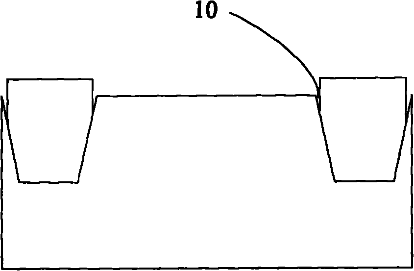
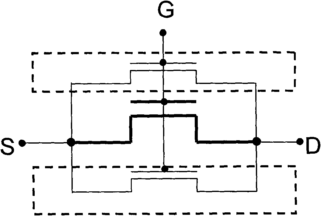
[0021] In the prior art, in the manufacturing process of MOS transistors, the size of the active region is larger than the predetermined size due to the recess phenomenon at the edge of the formed shallow trench isolation structure. As a result, two parasitic transistors with relatively low threshold voltages are connected in parallel on both sides of the subsequently formed transistor near the junction of the semiconductor substrate and the shallow trench isolation structure. During the operation of the transistor, a more serious anti-narrow channel effect will occur. The threshold voltage of the transistor decreases rapidly as the channel width decreases.

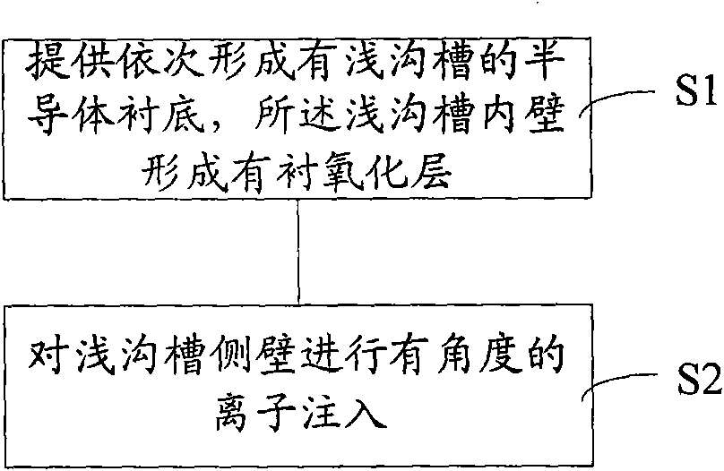
[0022] The present invention provides a method for improving the reverse narrow channel effect, such as image 3 As shown, step S1 is performed to provide a semiconductor substrate sequentially formed with shallow trenches, and a liner oxide layer is formed on the inner walls of the shallow trenches; step S2 is performed ...


PUM


Abstract

The invention provides methods for improving a reverse narrow channel effect and manufacturing a metal oxide semiconductor (MOS) transistor. The method for improving the reverse narrow channel effect comprises the following steps of: providing a semiconductor substrate on which shallow trenches are formed in turn; forming a lining oxide layer on the inner wall of each shallow trench; and performing angular ion implantation on the side wall of the shallow trench. By the method, the reverse narrow channel effect of the MOS transistor is effectively improved.

Description

technical field [0001] The invention relates to the manufacturing field of semiconductor devices, in particular to a method for improving the anti-narrow channel effect in the process of manufacturing MOS transistors. Background technique [0002] As the semiconductor industry develops towards smaller and faster devices, the feature lateral dimensions and depths of semiconductor devices are gradually reduced, requiring source / drain and source / drain extensions to be correspondingly shallower. Currently, the source / drain junction is almost always formed by doping by ion implantation. As the size of electronic components shrinks, how to manufacture the source and drain of metal-oxide-semiconductor (MOS) transistors with nanometer process technology is the development direction of ion implantation technology at present and in the future. [0003] However, with the shortening of the gate length, many negative effects that affect the normal operation of the transistor appear duri...

Claims


Application Information

Patent Timeline
Patent Type & Authority Applications(China)
IPC IPC(8): H01L21/762H01L21/265H01L21/336
Inventor 陈亮杨林宏
Owner SEMICON MFG INT (SHANGHAI) CORP
Why Eureka
Try Eureka