
MOS field effect pipe and its production

A technology of field effect transistors and low-voltage transistors, which is applied in the field of MOS field effect transistors and its production, and can solve problems such as transistor threshold voltage drop

Active Publication Date: 2007-06-20
SHANGHAI HUAHONG GRACE SEMICON MFG CORP
View PDF0 Cites 5 Cited by
  • Summary
  • Abstract
  • Description
  • Claims
  • Application Information

AI Technical Summary

Problems solved by technology

Therefore, this reverse narrow channel effect will cause the threshold voltage of the transistor to drop

Method used


Image

  • MOS field effect pipe and its production
  • MOS field effect pipe and its production

Examples


Embodiment Construction

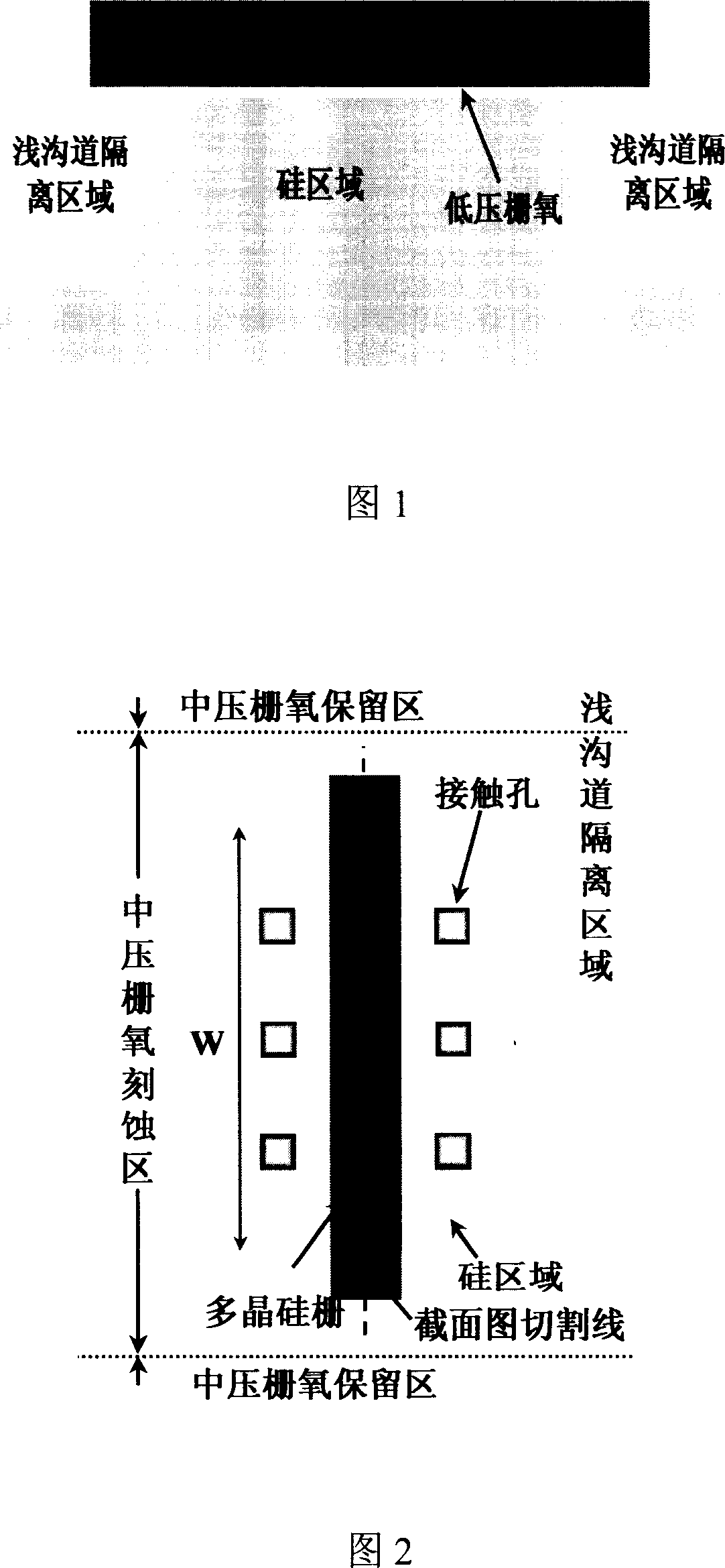
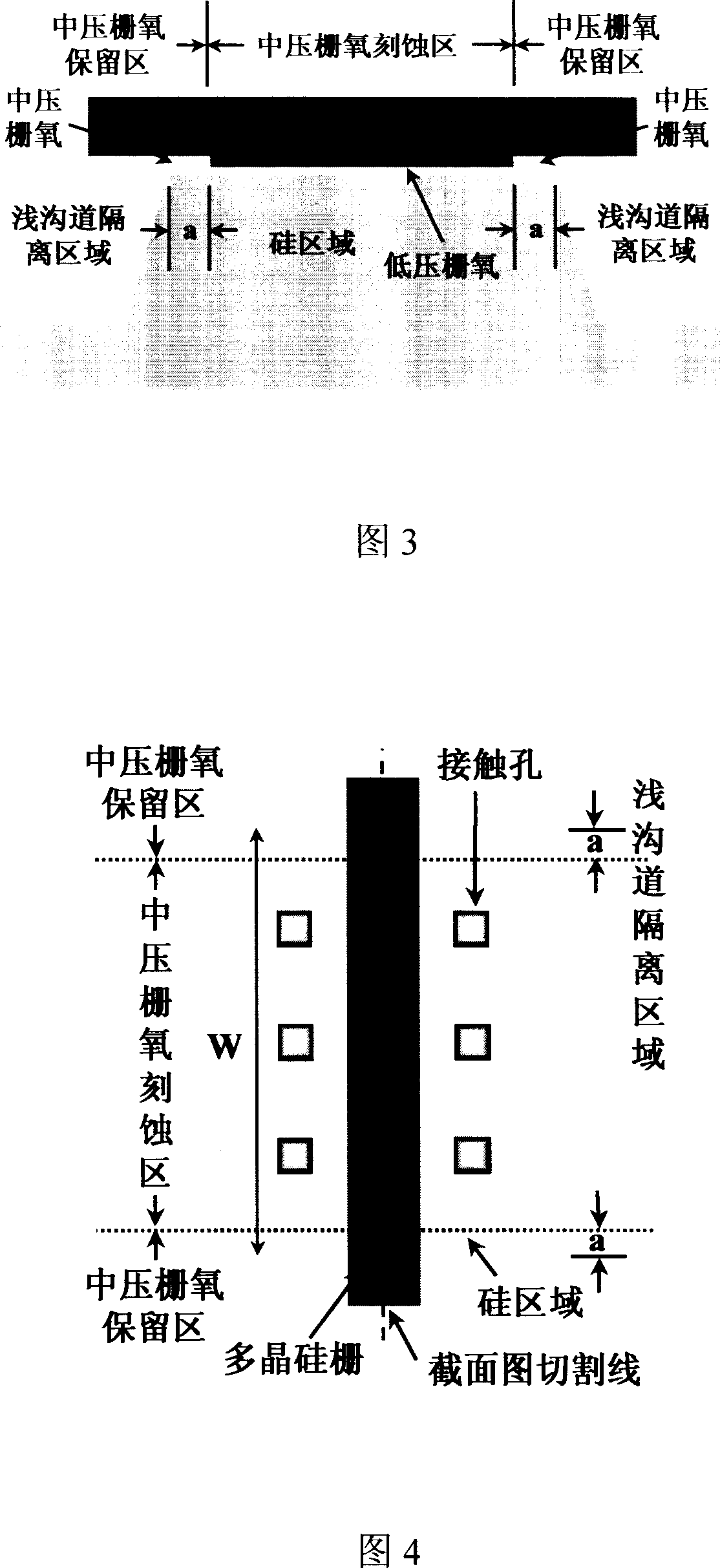
[0013] Fig. 3 is a schematic diagram of the cross-sectional structure of the MOS field effect transistor of the present invention. As shown in FIG. 3 , the MOS field effect transistor of the present invention has shallow trench isolation regions on both sides of the silicon region, a gate oxide on the top, and a polysilicon gate on the top of the gate oxide. Since the medium-voltage gate oxide in the middle of the silicon region is etched during the double gate oxide etching step, only the low-voltage gate oxide exists in the middle of the silicon region. And in the silicon region near the junction of the shallow trench isolation region and the silicon region, the distance from the junction of the shallow trench isolation region and the silicon region is a to the place of the junction, in the double gate oxide etching step The medium-voltage gate oxide is not etched, so that this part of gate oxide includes low-voltage gate oxide and medium-voltage gate oxide. Therefore, the ...


PUM


Abstract

The invention is concerned with a kind of MOS field-effect transistor. The thickness of gate oxide from the someplace of the simple channel insulated area closed to both sides of breadth and the silicon area on boundary of silicon area to simple channel insulated area and silicon area on boundary of silicon area is less than the thickness of gate oxide of the middle area of MOS transistor. The invention is also concerned with the production method of MOS field-effect transistor. During the etching step of double gate oxide, etch off the middle press thick gate oxide of the middle part of silicon area to MOS transistor and keep the middle press thick gate oxide from the someplace of the simple channel insulated area closed to both sides of breadth and the silicon area on boundary of silicon area to simple channel insulated area and silicon area on boundary of silicon area. It advances the threshold voltage to main transistor of low voltage MOS field-effect transistor and improves the problem about the descendent of threshold voltage coming from the anti-narrow channel effect of MOS field-effect transistor by keeping the middle press thick gate oxide of the rim of silicon area to low voltage MOS transistor.

Description

technical field [0001] The invention relates to the technical field of semiconductors, in particular to a MOS field effect transistor and a manufacturing method thereof. Background technique [0002] In the existing process for manufacturing MOS field effect transistors, the double gate oxide etching step completely etches away the medium-voltage thick gate oxide in the entire low-voltage MOS transistor region. FIG. 1 is a schematic diagram of a cross-sectional structure of a MOS field effect transistor in the prior art. As shown in FIG. 1, there are shallow trench isolation regions on both sides of the silicon region, a gate oxide on the top, and a polysilicon gate on the top of the gate oxide. The gate oxide of the MOS field effect transistor in the prior art is uniform in the width direction of the transistor. FIG. 2 is a schematic diagram of a layout of a MOS field effect transistor in the prior art. As shown in FIG. 2 , in the W direction, the thickness of the gate ox...

Claims


Application Information

Patent Timeline
IPC IPC(8): H01L29/78H01L29/40H01L21/336H01L21/28H01L21/316
Inventor 伍宏陈晓波
Owner SHANGHAI HUAHONG GRACE SEMICON MFG CORP
Learn More