MOS field effect pipe and its production

A technology of field effect transistors and silicon regions, applied in semiconductor/solid-state device manufacturing, electrical components, circuits, etc., can solve problems such as transistor threshold voltage drop, achieve the effect of increasing threshold voltage and improving anti-narrow channel effect

Active Publication Date: 2008-12-24
SHANGHAI HUAHONG GRACE SEMICON MFG CORP
View PDF6 Cites 0 Cited by
  • Summary
  • Abstract
  • Description
  • Claims
  • Application Information

AI Technical Summary

Problems solved by technology

Therefore, this reverse narrow channel effect will cause the threshold voltage of the transistor to drop

Method used


Image

  • MOS field effect pipe and its production
  • MOS field effect pipe and its production
  • MOS field effect pipe and its production

Examples


Embodiment Construction

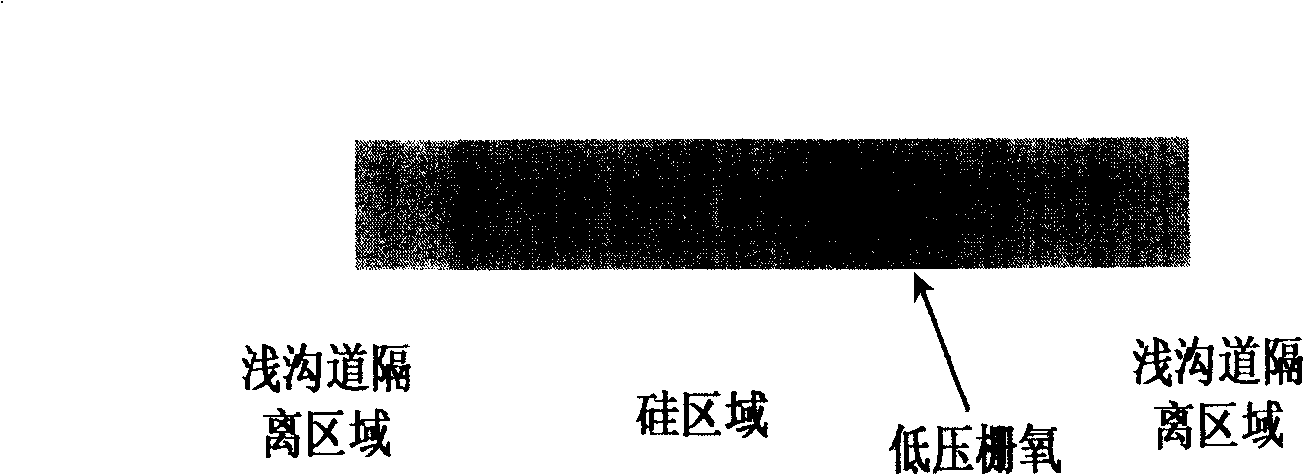
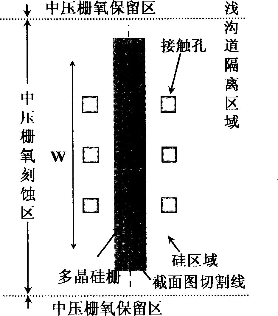
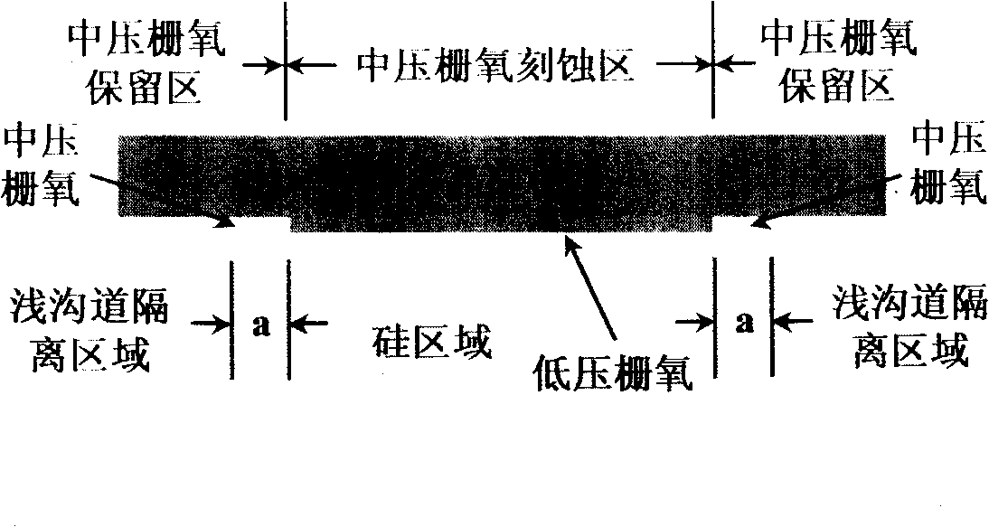
[0012] In a method for manufacturing a MOS field effect transistor of the present invention, the thick gate oxide of the medium voltage transistor must be grown after the thin gate oxide of the low voltage transistor is grown. Firstly, according to the severity of the anti-narrow channel effect of the low-voltage transistor, the thickness of the gate oxide of the medium-voltage transistor, the thickness of the gate oxide of the low-voltage transistor, the comprehensive device characteristics of the low-voltage transistor, and the relevant layout design rules are used to characterize the medium-voltage thick gate oxide. The geometry parameter "a" is optimized for the dimensions of the silicon edge region of the preserved low-voltage MOS transistor.

[0013] After the parameter "a" is determined, corresponding modifications are made to the layout of the double gate oxide etching photoresist. In the double gate oxide etching, only the medium-voltage thick gate oxide in the middle...


PUM


Abstract

The invention discloses a method for manufacturing a MOS field effect transistor. In the double gate oxide etching step, only the medium-voltage thick gate oxide in the middle part of the silicon region of the low-voltage MOS tube is etched away, and the two ends in the width direction of the MOS tube are kept close to the From somewhere within the silicon region at the junction of the shallow trench isolation region and the silicon region to a medium voltage thick gate oxide at the junction of the shallow trench isolation region and the silicon region. The invention improves the threshold voltage of the total transistor of the low-voltage MOS field effect transistor by retaining the medium-voltage thick gate oxide at the edge of the silicon region of the low-voltage MOS transistor, and improves the problem of threshold voltage drop caused by the reverse narrow channel effect of the MOS field effect transistor.

Description

technical field [0001] The invention relates to the technical field of semiconductors, in particular to a method for manufacturing a MOS field effect transistor. Background technique [0002] In the existing process for manufacturing MOS field effect transistors, the double gate oxide etching step completely etches away the medium-voltage thick gate oxide in the entire low-voltage MOS transistor region. figure 1 It is a schematic diagram of a cross-sectional structure of a MOS field effect transistor in the prior art. Such as figure 1 As shown, there are shallow trench isolation regions on both sides of the silicon region, the gate oxide is above the gate oxide, and the polysilicon gate is above the gate oxide. The gate oxide of the MOS field effect transistor in the prior art is uniform in the width direction of the transistor. figure 2 It is a schematic diagram of a layout of a MOS field effect transistor in the prior art. Such as figure 2 As shown, in the W directio...

Claims


Application Information

Patent Timeline
Patent Type & Authority Patents(China)
IPC IPC(8): H01L29/78H01L29/40H01L21/336H01L21/28H01L21/316
Inventor 伍宏陈晓波
Owner SHANGHAI HUAHONG GRACE SEMICON MFG CORP
Why Eureka
Try Eureka