MOS field effective pipe and its production

A technology of field effect transistor and channel direction, which is applied in semiconductor/solid-state device manufacturing, electrical components, circuits, etc., and can solve problems such as transistor threshold voltage drop

Inactive Publication Date: 2007-06-20
SHANGHAI HUA HONG NEC ELECTRONICS
View PDF0 Cites 2 Cited by
  • Summary
  • Abstract
  • Description
  • Claims
  • Application Information

AI Technical Summary

Problems solved by technology

Therefore, this reverse narrow channel effect will cause the threshold voltage of the transistor to drop

Method used


Image

  • MOS field effective pipe and its production
  • MOS field effective pipe and its production

Examples


Embodiment Construction

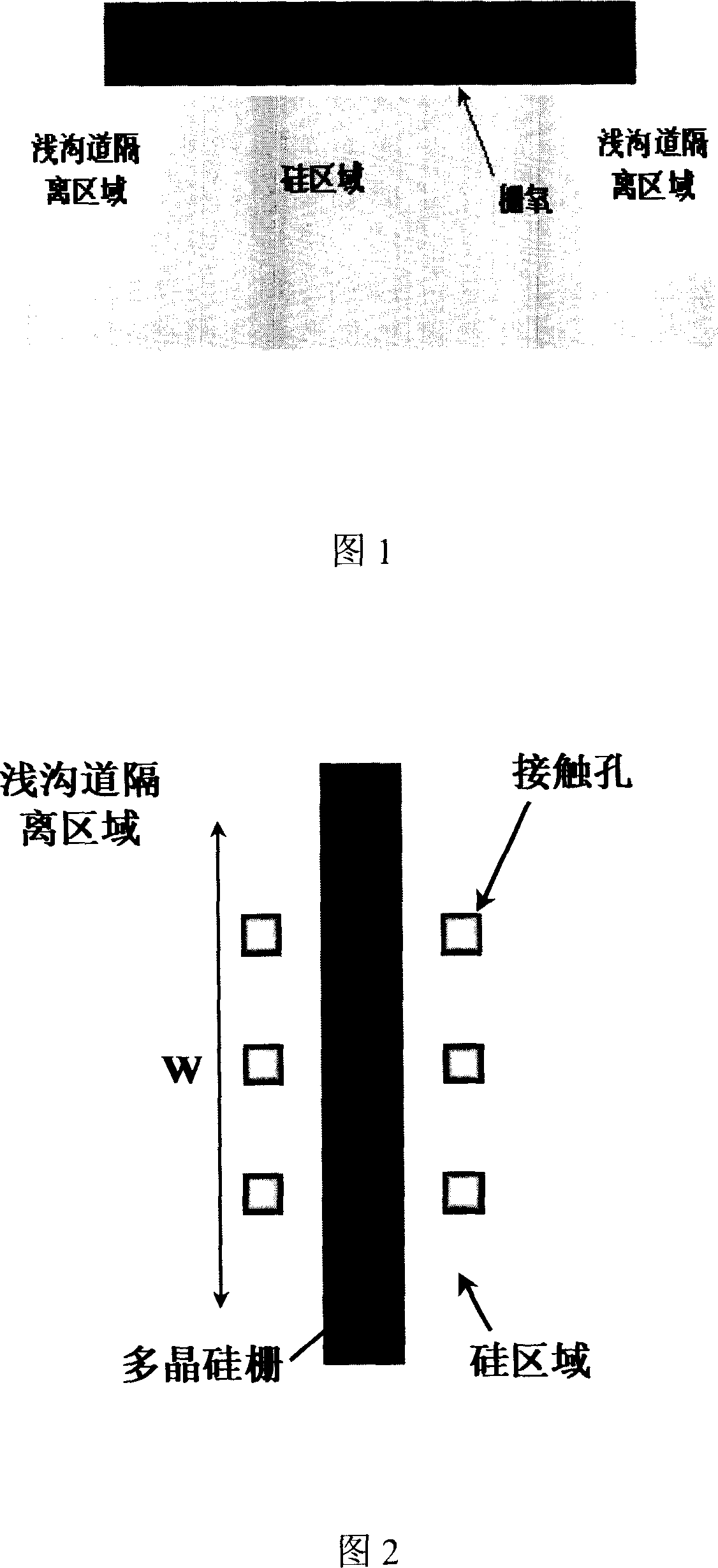
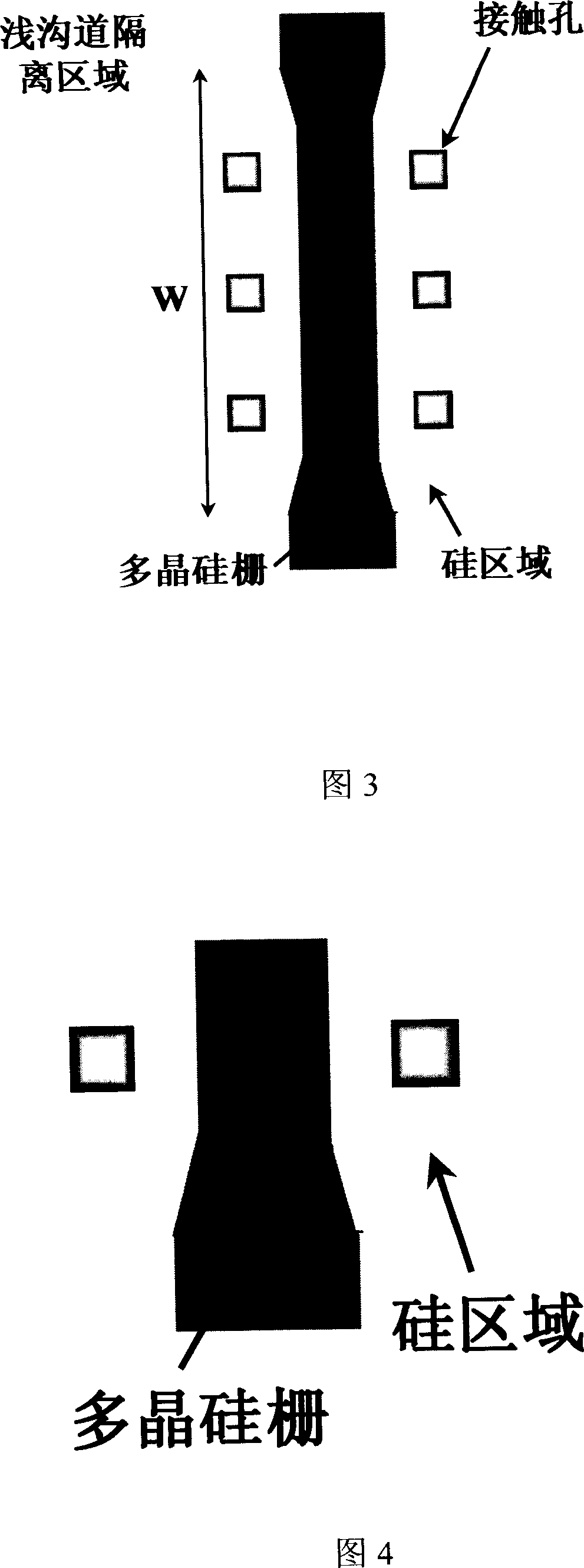
[0013] FIG. 3 is a schematic diagram of a layout of a MOS field effect transistor according to the present invention. A MOS field effect transistor of the present invention has a shallow trench isolation region on both sides of the silicon region, a gate oxide on the top, and a polysilicon gate on the top of the gate oxide. As shown in Figure 3, the width of the polysilicon gate of the MOS field effect transistor, in the W direction, is from somewhere in the silicon region close to the junction of the silicon region and the shallow trench isolation region to the junction of the silicon region and the shallow trench isolation region increases linearly. Fig. 4 is a partial enlarged view of the schematic diagram of the layout of the MOS field effect transistor of the present invention. As shown in Figure 4, the width of the polysilicon gate at the position of length b in the silicon region at the junction of the silicon region and the shallow trench isolation region is wider tha...


PUM


Abstract

The invention is concerned with a kind of MOS field-effect transistor. The breadth of the poly gate to MOS field-effect transistor adds in linearity from the someplace of the simple channel insulated area closed to both sides of breadth and the silicon area on boundary of silicon area. The invention is also concerned with the production method of MOS field-effect transistor. At first, define the geometry parameter of the shape change to this poly gate, according to the degree of anti-narrow channel effect and the general characteristic of MOS field-effect transistor. Then, change domain according to the decided geometry parameter. It adds the breadth of the poly gate on the rim of field-effect transistor in linearity, and this is equal to add the length of channel to parasitical transistor and reduces its leakage current to advance the threshold voltage of parasitical transistor. Then the result is to reduce the leakage current of main and advance its threshold voltage and solve the problem that the descendant of threshold voltage caused from the improvement of anti-narrow channel effect of MOS field-effect transistor.

Description

technical field [0001] The invention relates to the technical field of semiconductors, in particular to a MOS field effect transistor and a manufacturing method thereof. Background technique [0002] FIG. 1 is a schematic diagram of a cross-sectional structure of a MOS field effect transistor in the prior art. As shown in FIG. 1 , on both sides of the silicon region are shallow trench isolation regions, above which is a gate oxide, and above the gate oxide is a polysilicon gate. In the current conventional MOS field effect transistor, the width of the polysilicon gate is uniform in the width direction of the field effect transistor. FIG. 2 is a schematic diagram of a layout of a MOS field effect transistor in the prior art. As shown in FIG. 2 , in the W direction, that is, in the width direction of the field effect transistor, the width of the polysilicon gate is uniform. [0003] In MOS field effect transistors using shallow trench isolation (STI) technology in the prior...

Claims


Application Information

Patent Timeline
Patent Type & Authority Applications(China)
IPC IPC(8): H01L29/78H01L21/336
Inventor 伍宏陈晓波
Owner SHANGHAI HUA HONG NEC ELECTRONICS
Why Eureka
Try Eureka