Method to improve SRAM performance and stability

a technology of sram and stability, applied in the field of semiconductor device manufacturing, can solve the problems of reducing width and length, unable to accommodate about one hundred or fewer, and may persist with shrinking semiconductor devices, so as to achieve faster operation, reduce transistor width, and improve reliability

Active Publication Date: 2007-03-13
TEXAS INSTR INC
View PDF20 Cites 132 Cited by
  • Summary
  • Abstract
  • Description
  • Claims
  • Application Information

AI Technical Summary

Benefits of technology

[0005]Issues may persist with shrinking semiconductor devices. For example, random dopant fluctuation, and associated disadvantageous effects resulting therefrom, may become more prevalent as transistor widths and lengths are reduced. In general, random dopant fluctuation refers to differences in the amount of dopant atoms received within certain areas (e.g., source / drain regions and / or upper portion of gate structure) as those areas are reduced in size. For example, even the most uniform application of dopant atoms may produce a difference of a few atoms within targeted areas where the respective sizes of those areas are so small that they can only be expected to accommodate about one hundred or fewer dopant atoms. In such small areas, a difference of just a few dopant atoms can cause the areas to have different electrical properties. This can, for example, cause respective transistors which are formed from one or more of these areas to have different operating characteristics. For example, a plurality of transistors that are supposed to be ‘matched’ may trigger on or off at different threshold voltages (Vt). It can be appreciated that the effects of RDF may be even more noticeable in certain types of semiconductor devices, such as static random access memory (SRAM), for example, which incorporate multiple transistors.
[0006]Semiconductor memories can, for example, be characterized as volatile random access memories (RAMS) or nonvolatile read only memories (ROMs), where RAMs can either be static (SRAM) or dynamic (DRAM) differing mainly in the manner by which they store a state of a bit. In SRAM, for example, each memory cell includes transistor-based circuitry that implements a bistable latch, which relies on transistor gain and positive (e.g., reinforcing) feedback so that it can only assume one of two possible states, namely on (state 1) or off (state 2). The latch can only be programmed or induced to change from one state to the other through the application of a voltage or other external stimuli. This arrangement is desirable for a memory cell since a state written to the cell will be retained until the cell is reprogrammed. DRAMs on the other hand implement a capacitor that is either charged or discharged to store the on (state 1) or off (state 2) state of a cell. Capacitors discharge over time, however, and DRAMs must therefore be periodically ‘refreshed’. Also, a bistable latch can generally be switched between states much faster than the amount of time it takes to charge or discharge a capacitor. Thus, SRAMs are generally more reliable and operate faster than DRAMs. Accordingly, SRAMs are a desirable type of memory for certain types of applications.
[0007]SRAM is typically arranged as a matrix of memory cells fabricated in an integrated circuit chip, and address decoding in the chip allows access to each cell for read / write functions. SRAM memory cells use active feedback in the form of cross-coupled inverters to store a bit of information, and the cells are often arranged in rows so that blocks of data such as words or bytes can be written or read simultaneously. Standard SRAM memory cells have many variations. The basic CMOS SRAM cell generally includes two N-type (NMOS) pull-down or drive transistors and two P-type (PMOS) load transistors in a cross-coupled inverter configuration, with two additional NMOS select transistors added to make up a six-transistor cell. Additionally, application specific SRAM cells can include an even greater number of transistors. Since a plurality of transistors are utilized in SRAM, and since random dopant fluctuations may become more prevalent as transistor widths are reduced, the adverse effects of random dopant fluctuations may present themselves to a great degree in SRAM, particularly as that type of memory is continually scaled down.
[0008]Accordingly, it would be desirable to have a technique that would allow transistors to be scaled down while mitigating RDF, particularly where the transistors may be used in SRAM.SUMMARY OF THE INVENTION
[0009]The following presents a simplified summary of the invention in order to provide a basic understanding of some aspects of the invention. This summary is not an extensive overview of the invention. It is intended neither to identify key or critical elements of the invention nor to delineate the scope of the invention. Rather, its primary purpose is merely to present one or more concepts of the invention in a simplified form as a prelude to the more detailed description that is presented later.
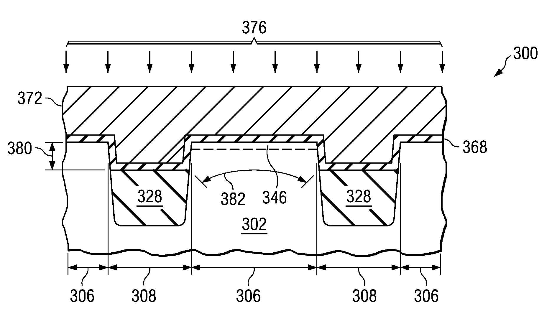
[0010]The present invention pertains to increasing the width of a transistor while the transistor itself may be scaled down in size. The transistor width is increased by forming recesses within shallow trench isolation (STI) regions adjacent to the transistor. The recesses provide a wraparound area that increases the width of the transistor and provides additional effective transistor area wherein more dopant atoms can be deposited. This increased dopant area facilitates a reduction in random dopant fluctuation (RDF). In this manner transistors formed in accordance with one or more aspects of the present invention may yield improved performance when incorporated into SRAM since the probability is increased that such transistors will be more closely matched.

Problems solved by technology

Issues may persist with shrinking semiconductor devices.
For example, random dopant fluctuation, and associated disadvantageous effects resulting therefrom, may become more prevalent as transistor widths and lengths are reduced.
For example, even the most uniform application of dopant atoms may produce a difference of a few atoms within targeted areas where the respective sizes of those areas are so small that they can only be expected to accommodate about one hundred or fewer dopant atoms.

Method used


Image

  • Method to improve SRAM performance and stability
  • Method to improve SRAM performance and stability
  • Method to improve SRAM performance and stability

Examples


Embodiment Construction

[0016]One or more aspects of the present invention are described with reference to the drawings, wherein like reference numerals are generally utilized to refer to like elements throughout, and wherein the various structures are not necessarily drawn to scale. In the following description, for purposes of explanation, numerous specific details are set forth in order to provide a thorough understanding of one or more aspects of the present invention. It may be evident, however, to one skilled in the art that one or more aspects of the present invention may be practiced with a lesser degree of these specific details. In other instances, known structures and devices are shown in block diagram form in order to facilitate describing one or more aspects of the present invention.

[0017]The present invention pertains to increasing the width of a transistor by over etching shallow trench isolation (STI) structures. For a given layout footprint, the over etched STI structures provide additiona...


PUM


Abstract

A technique is disclosed for increasing the width of a transistor (300) while the transistor itself may be scaled down. The transistor width (382) is increased by forming recesses (352) within shallow trench isolation (STI) regions (328) adjacent to the transistor (300). The recesses (352) provide an area that wraps around the transistor and thereby increases the width (382) of the transistor (300). This wraparound area provides additional space for dopant atom deposition, which facilitates a reduction in random dopant fluctuation (RDF). In this manner, transistors formed in accordance with one or more aspects of the present invention, may yield improved performance when incorporated into SRAM since the probability that such transistors will be more closely matched is increased.

Description

FIELD OF INVENTION[0001]The present invention relates generally to semiconductor processing, and more particularly to fabricating a transistor in a manner that increases active width to mitigate random dopant fluctuation (RDF) and thereby facilitate improved performance and stability, particularly when utilized in static random access memory (SRAM).BACKGROUND OF THE INVENTION[0002]Several trends presently exist in the semiconductor and electronics industry. Devices are continually being made smaller, faster and requiring less power. One reason for these trends is that more personal devices are being fabricated that are relatively small and portable, thereby relying on a battery as their primary supply. For example, cellular phones, personal computing devices, and personal sound systems are devices that are in great demand in the consumer market. In addition to being smaller and more portable, personal devices are also requiring increased memory and more computational power and speed...

Claims


Application Information

Patent Timeline
Patent Type & Authority Patents(United States)
IPC IPC(8): H01L21/76
CPCG11C11/412H01L27/1104H01L27/11H10B10/00H10B10/12
Inventor WU, ZHIQIANGYU, SHAOFENGCLEAVELIN, C. RINN
Owner TEXAS INSTR INC
Why Eureka
Try Eureka