Liquid crystal display device panel and manufacturing method thereof

A technology of liquid crystal display device and manufacturing method, which is applied in the direction of instruments, nonlinear optics, optics, etc., can solve the problem that the thickness of the cell is difficult to select the transmittance, etc., achieve good transmittance of the liquid crystal cell, optimize the average optical retardation value, and realize The effect of wide viewing angle

Active Publication Date: 2013-01-09
SHANGHAI TIANMA MICRO ELECTRONICS CO LTD
View PDF0 Cites 0 Cited by
  • Summary
  • Abstract
  • Description
  • Claims
  • Application Information

AI Technical Summary

Problems solved by technology

[0005] In the existing MVA mode liquid crystal display device, in a single pixel area, the ratio of the area of ​​the protrusion / inclined surface on the substrate to the total display area is usually less than 50%, making it difficult to select the cell thickness for the R, G, and B areas in the pixel. for the best transmittance

Method used


Image

  • Liquid crystal display device panel and manufacturing method thereof
  • Liquid crystal display device panel and manufacturing method thereof
  • Liquid crystal display device panel and manufacturing method thereof

Examples


Embodiment Construction

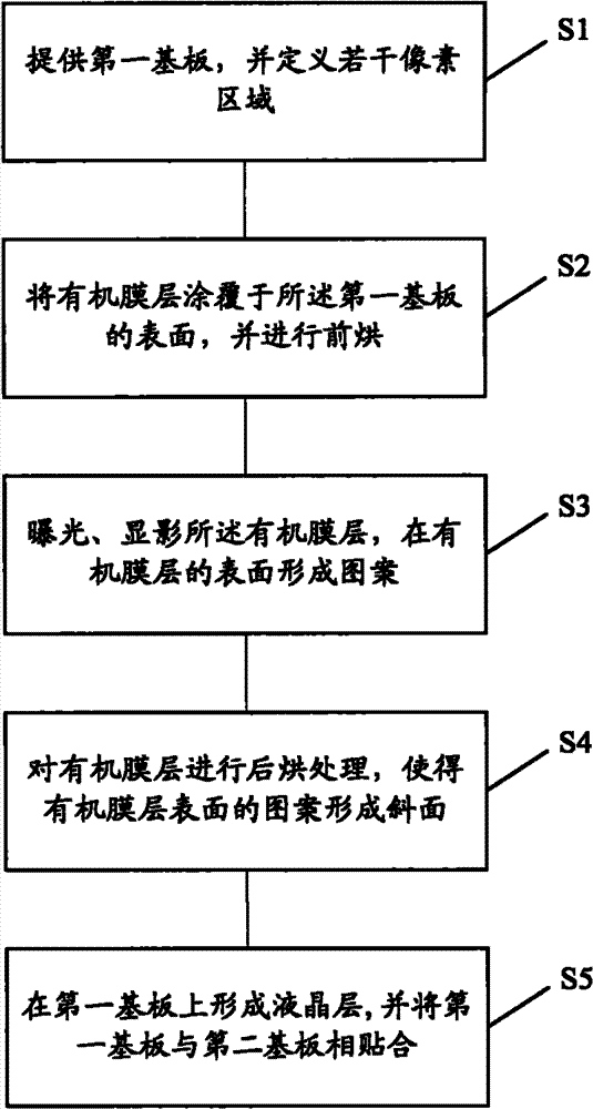
[0034] The specific embodiments of the present invention will be further introduced in conjunction with the accompanying drawings.

[0035] The smallest display unit of a liquid crystal display is a pixel. Therefore, the panel of the liquid crystal display device includes a pixel array, so the panel of the liquid crystal display device can be divided into several pixel regions, and the pixel regions are separated by data lines and scan lines.

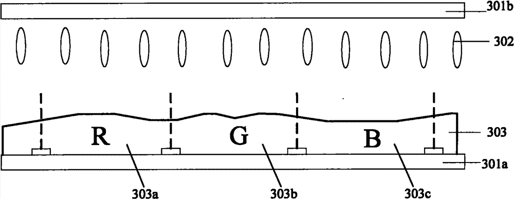
[0036] Such as figure 1 Shown is a schematic structural view of a single pixel region of the liquid crystal display panel of the present invention, and the liquid crystal display panel includes:

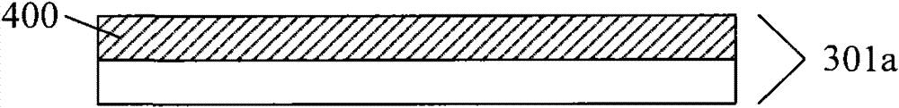
[0037] The first substrate 301a; the second substrate 301b; the organic film layer 303, located on the side of the first substrate 301a facing the second substrate 301b;

[0038] The liquid crystal layer 302 is located between the first substrate 301a and the second substrate 301b;

[0039] A single pixel can also be divided into multiple su...


PUM

PropertyMeasurementUnit
thicknessaaaaaaaaaa
thicknessaaaaaaaaaa
thicknessaaaaaaaaaa

Abstract

The invention provides an MVA (Multi-domain Vertical Alignment)-mode liquid crystal display device panel and a manufacturing method thereof. The panel comprises a first substrate, a second substrate, an organic membrane layer and a liquid crystal layer, wherein the first substrate comprises pixel regions defined by data lines and scanning lines on the first substrate; the organic membrane layer is positioned at the side of the first substrate, which faces to the second substrate; the surface of the organic membrane layer, which faces to the second substrate, is provided with an inclined surface; the liquid crystal layer is positioned between the first substrate and the second substrate; when a pressure is not applied, liquid crystal molecules in the liquid crystal layer are arranged to beperpendicular to the surface of the organic membrane layer close to the liquid crystal layer; and in one single pixel region, the ratio of the area of the inclined plane of the organic membrane layerto the single pixel area is more than 50 percent. In the invention, by regulating the thickness of the organic membrane layer and the thickness of a liquid crystal box, average optical retardation values corresponding to R, G and B are effectively optimized so that the wide viewing angle and the good transmissivity of the liquid crystal box are realized.

Description

technical field [0001] The invention relates to the field of liquid crystal manufacturing, in particular to an MVA mode liquid crystal display panel and a manufacturing method thereof. Background technique [0002] Liquid crystal display devices are widely used in handheld information exchange terminals and various display fields because of their low space occupation rate and low energy consumption. The liquid crystal display device controls the alignment direction of liquid crystal molecules when the light from the light source passes through the liquid crystal layer through an electric field, and changes the transmittance to display images. According to different specific principles, the liquid crystal display device has developed from the early TN mode to the current VA mode and IPS mode. [0003] In the vertical alignment (VA) mode, the liquid crystal molecules are vertically arranged in the liquid crystal layer in the liquid crystal cell relying on the surface anchor e...

Claims


Application Information

Patent Timeline
Patent Type & Authority Patents(China)
IPC IPC(8): G02F1/1333
Inventor 马骏罗熙曦吴勇李忠丽
Owner SHANGHAI TIANMA MICRO ELECTRONICS CO LTD
Why Eureka
Try Eureka