Check patentability & draft patents in minutes with Patsnap Eureka AI!

Output element, signal rotation rate correcting method and amplitude control method

A technology of output components and slew rate, applied in the direction of logic circuit connection/interface layout, etc., can solve the problems of waveform distortion, parasitic capacitance reducing the overall circuit operation speed, waveform interleaving distortion, etc.

Active Publication Date: 2013-03-06
IND TECH RES INST
View PDF0 Cites 0 Cited by
  • Summary
  • Abstract
  • Description
  • Claims
  • Application Information

AI Technical Summary

Problems solved by technology

In order to reduce the voltage difference between the two, it is necessary to increase the size of the inverter, that is, to reduce the voltage difference passing through the inverter, and the increase in parasitic capacitance due to the increase in area will reduce the operating speed of the overall circuit
In addition, the on-resistance of the inverter will produce a non-linear effect with the difference in the output voltage to the load, which will greatly distort the output waveform, and the dead time control of PMOS and NMOS may also Will cause interlacing distortion of the waveform
Therefore, the slew rate control device of the existing output signal based on the switching inverter has many disadvantages.

Method used


Image

  • Output element, signal rotation rate correcting method and amplitude control method
  • Output element, signal rotation rate correcting method and amplitude control method
  • Output element, signal rotation rate correcting method and amplitude control method

Examples


Embodiment Construction

[0037] Those discussed below are preferred embodiments of the invention. Although the description is based on the spirit of the present invention with the following examples, it is not intended to limit the present invention to these examples. The examples given in the present invention are only used for illustration of this specification, and are not intended to limit the viewpoint of the present invention.

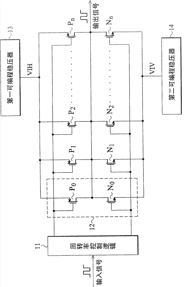
[0038] figure 2 It is a schematic diagram of an embodiment of an output element capable of controlling signal slew rate and amplitude in the present invention. In this embodiment, a test device is used to output a test signal to a device under test (device under test) as an example. Therefore, the input signal refers to the test signal output by the original test device, and the output signal refers to the test signal after the slew rate and voltage. The measured signal is leveled and sent to the object under test or the load through the isolated drive circuit, and th...


PUM


Abstract

The invention discloses an output element capable of outputting a drive signal with accurately controllable rotation rate and voltage level under different loads and continuously changed load conditions. By utilizing a precise control and adjusting circuit through a self-correction program, the precision of an output waveform is improved, influences on production and manufacturing as well as working environment modification are reduced, and an isolated driving circuit is used for providing driving capacity and isolating outside load modification.

Description

technical field [0001] The invention discloses a component capable of controlling the slew rate and level output, which can output a drive signal with precisely controllable slew rate and voltage level under different loads and continuous changes in load conditions. Background technique [0002] The output and drive circuit is a common interface circuit in chip design. It is used as a buffer device between the core circuit of the chip and external circuits or other chips, which can reduce the impact of load variation and interference outside the chip. General output and drive circuits only need to have appropriate current drive capability and appropriate self-protection mechanism. However, because the output and the load device to be driven by the drive circuit may have great variation, and there is a very high accuracy requirement on the output waveform, such as the rise and fall time of the signal transition and the output level, as well as current implementation. [000...

Claims


Application Information

Patent Timeline
Patent Type & Authority Patents(China)
IPC IPC(8): H03K19/0175
Inventor 庄凯翔侯信宏李永斌
Owner IND TECH RES INST
Features
  • R&D
  • Intellectual Property
  • Life Sciences
  • Materials
  • Tech Scout
  • Unparalleled Data Quality
  • Higher Quality Content
  • 60% Fewer Hallucinations
Learn More