Method for detecting mechanical scratching condition of silicon wafers

A detection method and technology for silicon wafers, applied in the directions of optical testing flaws/defects, semiconductor/solid-state device testing/measurement, etc., can solve problems such as difficulty in judging the source machine, yield loss, and time-consuming detection methods, reducing Victimize batches, improve yield, avoid time-consuming and blind effects

Inactive Publication Date: 2011-07-20
SHANGHAI HUA HONG NEC ELECTRONICS
View PDF0 Cites 21 Cited by
  • Summary
  • Abstract
  • Description
  • Claims
  • Application Information

AI Technical Summary

Problems solved by technology

[0005] This detection method is time-consuming, and it is difficult to determine the source machine before repeated scratches
And the repeated occurrence of scratches means greater yield loss

Method used


Image

  • Method for detecting mechanical scratching condition of silicon wafers
  • Method for detecting mechanical scratching condition of silicon wafers
  • Method for detecting mechanical scratching condition of silicon wafers

Examples


Embodiment Construction

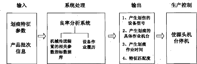
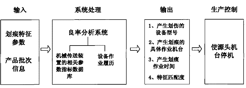
[0022] The method for detecting mechanical scratches on silicon wafers of the present invention uses the following steps to detect the source of mechanical scratches on silicon wafers:

[0023] 1. Establish the characteristic information database of the mechanical conveying device of the silicon wafer conveying device on the silicon wafer production line;

[0024] Since there are dozens of actual types and sizes of the manipulators of the mechanical transmission device, the scratch sizes caused by different types of manipulators are also different.

[0025] The mechanical transfer device includes all relevant parts (manipulators, conveyor belts, etc.) Detailed dimensions of possible scratches on the part;

[0026] 2. When mechanical scratches are detected on a certain batch of silicon wafers on the production line, the characteristic parameters of the silicon wafer scratches are collected, including the number of the scratched silicon wafers, the angle, length, and intercept ...


PUM


Abstract

The invention discloses a method for detecting the mechanical scratching condition of silicon wafers. A method for detecting source machines which are subjected to mechanical scratching comprises the following steps of: 1, establishing a characteristic information database of a mechanical transmission device of a silicon wafer carrying device on a silicon wafer production line; 2, when detecting that the silicon wafers are subjected to the mechanical scratching on the production line, collecting characteristic parameters of silicon wafer scratches; 3, comparing the characteristic parameters of the silicon wafer scratches with the characteristic information of the mechanical transmission device in the database to retrieve equipment models matched with the scratches; and 4, analyzing the equipment operating records of the silicon wafers, and screening specific operating machines with the scratches and operating time out. By the method, the source machines with the scratches can be found quickly, and machine halt can be performed as soon as possible when the silicon wafers are scratched to reduce damaged batches and the loss of the wafers and improve the yield.

Description

technical field [0001] The invention relates to a detection method in the manufacturing process of silicon wafers, in particular to a detection method for mechanical scratches of silicon wafers. Background technique [0002] In the production process of silicon wafers, it is necessary to use a precisely controlled conveying device to transport silicon wafers. During the transfer process, the manipulator of the transfer device only touches the back of the silicon wafer and does not touch the front of the silicon wafer, so as to avoid scratches on the silicon wafer. However, in the actual operation process, due to mechanical wear or loose screws, the manipulator will be displaced, and the distance between the silicon wafers is very narrow, so the displacement of the manipulator can easily cause the manipulator to touch the bottom during the movement. The surface of a silicon wafer, causing scratches on the silicon wafer, such as figure 1 shown. [0003] Once the mechanical ...

Claims


Application Information

Patent Timeline
Patent Type & Authority Applications(China)
IPC IPC(8): H01L21/66G01N21/88
Inventor 吴苑
Owner SHANGHAI HUA HONG NEC ELECTRONICS
Why Eureka
Try Eureka