
Improved main circuit structure of photovoltaic synchronization inverter
A main circuit, an improved technology, applied in the direction of photovoltaic power generation, single-network parallel feeding arrangement, electrical components, etc., can solve problems such as considerable impact
- Summary
- Abstract
- Description
- Claims
- Application Information
AI Technical Summary
Problems solved by technology
Method used
Image

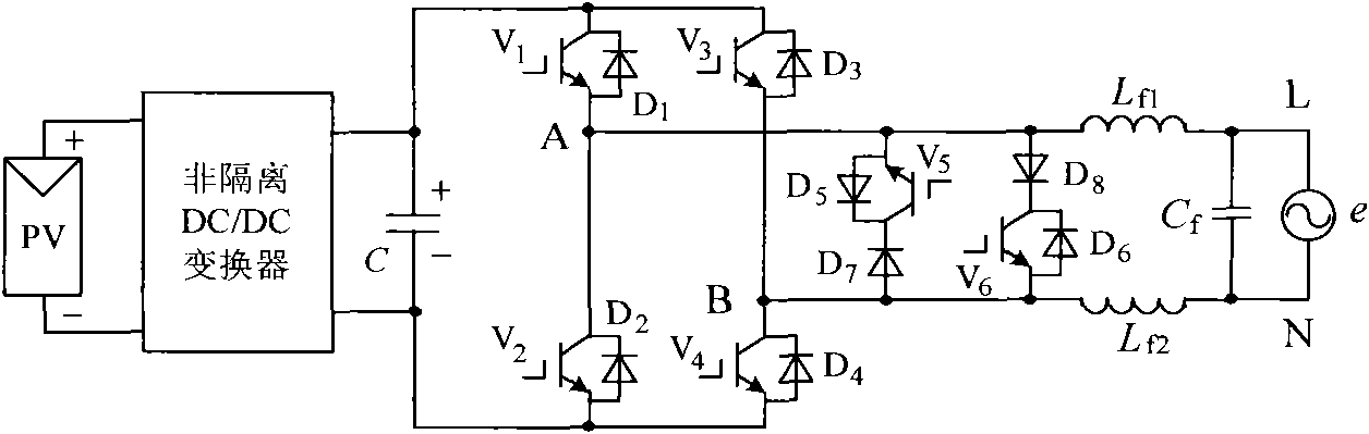
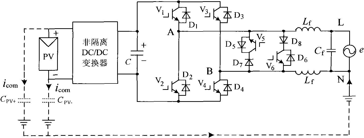
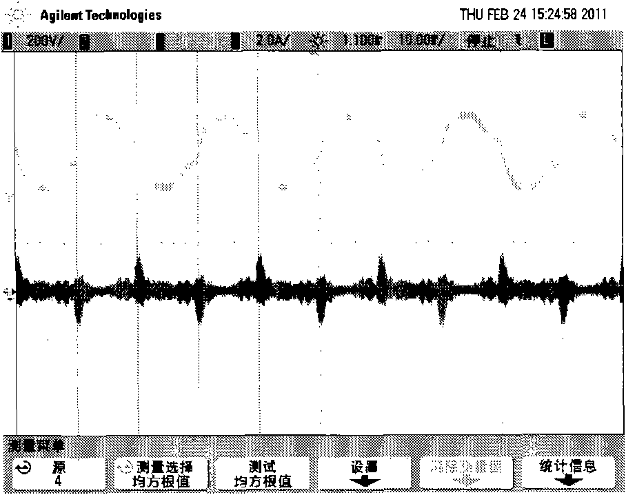
Examples
Embodiment 2
[0056] Such as Figure 13 Shown, L f1 The other end of the capacitor C f One end of the EMI filter is connected to node G; L f2 The other end of the capacitor C f The other end of the EMI filter is connected to the node H; one is connected by the capacitor C 3 、C 4 、C 5 、C 6 composed of H-bridge capacitor banks, where C 5 one end of the C 6 One end of the EMI filter, one output end of the EMI filter, and the L end of e are connected; C 3 one end of the C 4 One end of the EMI filter, the other output end of the EMI filter, the N end of e and the ground connection; C 5 the other end of the C 3 The other end of the PV is connected to the node C; C 6 the other end of the C 4 The other end of the PV and the negative pole of the PV are connected to the node D.
Embodiment 3
[0058] Such as Figure 14 Shown, L f1 the other end of the C f One end of e is connected to the L end of e; L f2 the other end of the C f The other end, the N end of e and the ground are connected; one is connected by the capacitor C 3 、C 4 、C 5 、C 6 composed of H-bridge capacitor banks, where C 5 one end of the C 6 end of the L f1 The other end is connected to the node L; C 3 one end of the C 4 end of the L f2 The other end of is connected to node N; C 5 the other end of the C 3 The other end of the PV is connected to the node C; C 6 the other end of the C 4 The other end of the PV and the negative pole of the PV are connected to the node D.
Embodiment 4
[0060] Such as Figure 15 Shown, L f1 the other end of the C f One end of the EMI filter and one input end of the EMI filter are connected to the node G; L f2 the other end of the C f The other end of the EMI filter and the other input end of the EMI filter are connected to node H; one output end of the EMI filter is connected to the L end of e; the other output end of the EMI filter is connected to the N end of e and the ground; by capacitance C 5 、C 6 composed of a half H-bridge capacitor bank, where C 5 one end of the C 6 end of the L f1 The other end is connected to node G; C 5 The other end of the PV is connected to the positive pole of the node C; C 6 The other end of the node is connected to the negative pole of PV at node D.
PUM
 Abstract
Description
Claims
Application Information