Static random access memory and implementation method thereof

A static random access and memory technology, applied in static memory, digital memory information, information storage, etc., can solve the problem of increasing chip size, reduce design cost, improve signal transmission quality, and reduce the number of layers of chip layout and wiring.

Inactive Publication Date: 2011-08-03
INSPUR BEIJING ELECTRONICS INFORMATION IND
View PDF4 Cites 3 Cited by
  • Summary
  • Abstract
  • Description
  • Claims
  • Application Information

AI Technical Summary

Problems solved by technology

[0002] With the rapid development of integrated circuit technology, in order to meet people's needs, high-performance microprocessors are often embedded with large-capacity static random access memory (SRAM). On the one hand, the increase in memory can build chips with more powerful performance, so as to better adapt to The application requirements of various chips today, but on the other hand, it is also caught in the dilemma of increasing chip size

Method used


Image

  • Static random access memory and implementation method thereof
  • Static random access memory and implementation method thereof
  • Static random access memory and implementation method thereof

Examples


Embodiment Construction

[0032] Embodiments of the present invention will be described in detail below in conjunction with the accompanying drawings.
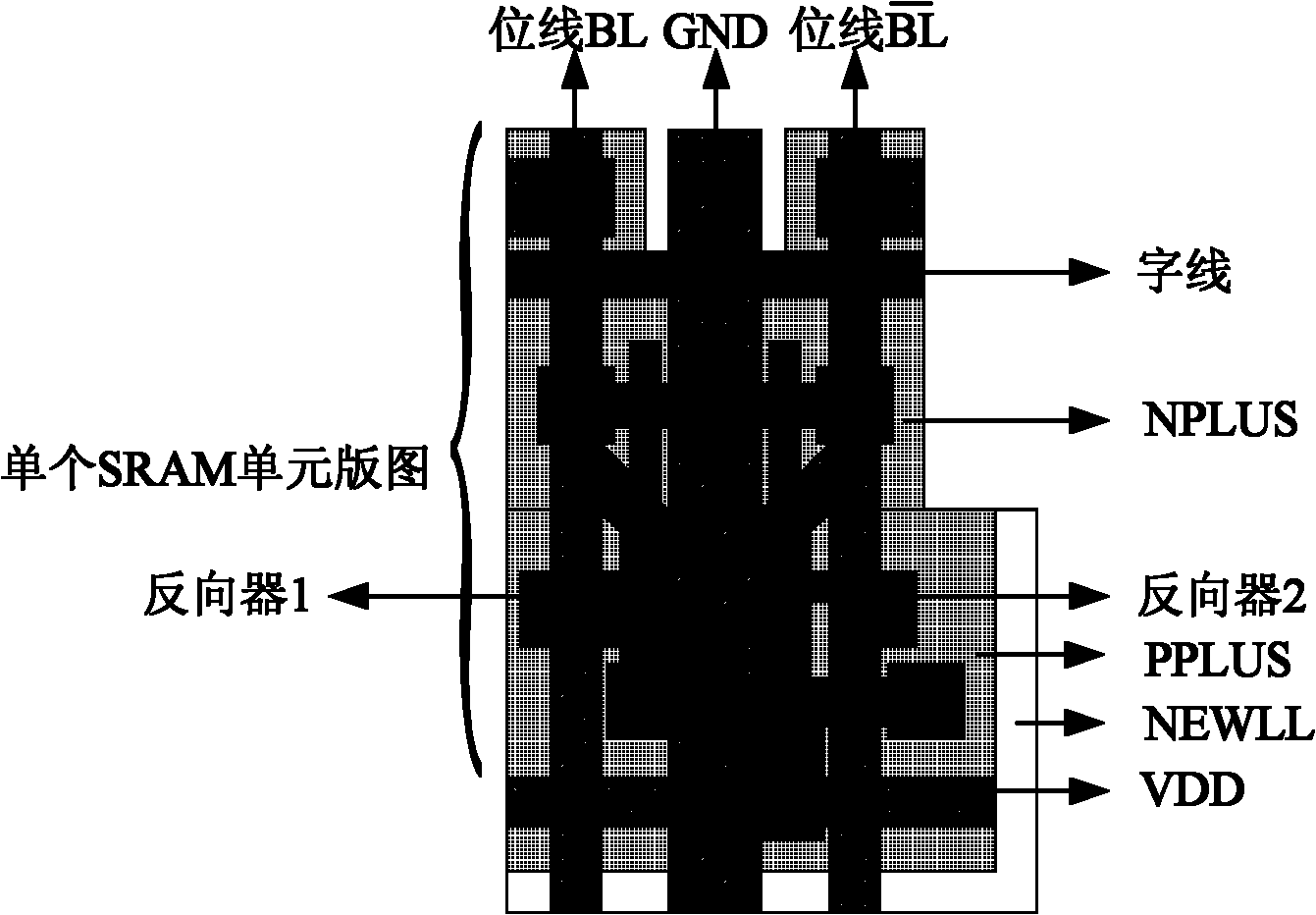
[0033] The area of ​​the large-capacity SRAM memory storage array determines the overall chip area of ​​the SRAM memory module, and even determines the area of ​​the entire chip. Therefore, in order to reduce the chip design area, the embodiments of the present invention preferably propose the implementation of using memory cell pairs, and The memory cell pair is used as the basic unit of the memory array, wherein the memory cell pair is formed by connecting every two memory cells so that the power lines of the two overlap, and the perforations of the power line overlap. Since the two storage units share one power supply line, the area of ​​one power supply VDD line and the space between two power supply lines are reduced. The design method of the storage unit pair greatly increases the integration density of the storage array, can effectively reduce t...


PUM


Abstract

The invention provides a static random access memory and an implementation method thereof. The static random access memory comprises a storage array. The storage array comprises a plurality of storage unit pairs; two storage units are included in each storage unit pair; power traces of the two storage units are superposed, and through holes of the power traces are superposed. The static random access memory can realize the high-density integration of the storage array, and reduces the design area and the design cost of a chip.

Description

technical field [0001] The invention relates to the field of integrated circuit design, in particular to a static random access memory and its realization method. Background technique [0002] With the rapid development of integrated circuit technology, in order to meet people's needs, high-performance microprocessors are often embedded with large-capacity static random access memory (SRAM). On the one hand, the increase in memory can build chips with more powerful performance, so as to better adapt to The application requirements of various chips today, but on the other hand, they are also caught in the dilemma of increasing chip size. Large-capacity memory and higher and higher integration density increase the number of chip design layers and make the manufacturing process more complex, and also increase the design density of chip units. More than 70% of the microprocessor chip area embedded with large-capacity memory is occupied by memory. Therefore, in order to reduce t...

Claims


Application Information

Patent Timeline
Patent Type & Authority Applications(China)
IPC IPC(8): G11C11/413
Inventor 王恩东胡雷钧李仁刚秦济龙
Owner INSPUR BEIJING ELECTRONICS INFORMATION IND
Why Eureka
Try Eureka