

TSV (through silicon via) chip bonding structure
A chip bonding and bonding structure technology, applied in the field of microelectronics, can solve problems such as non-solutions, and achieve the effect of preventing lateral offset and precisely aligning contacts
- Summary
- Abstract
- Description
- Claims
- Application Information
AI Technical Summary
Problems solved by technology
Method used
Image

Examples
Embodiment Construction
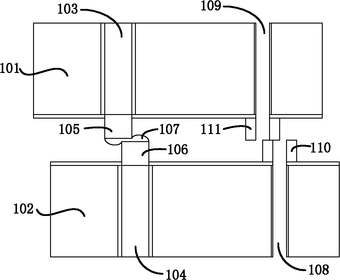
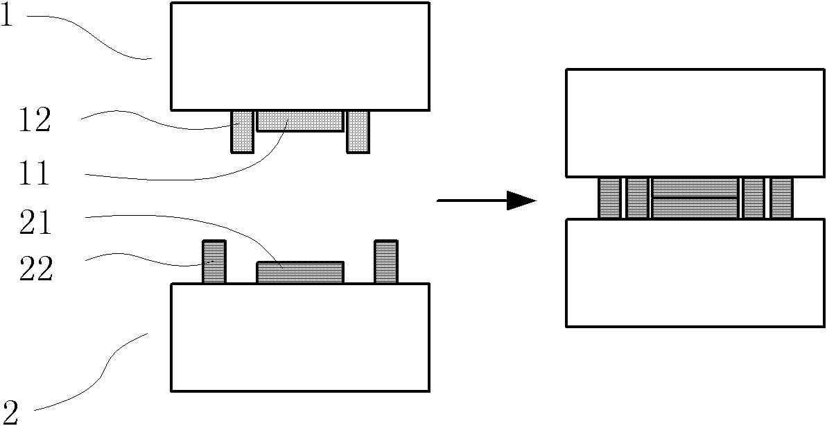
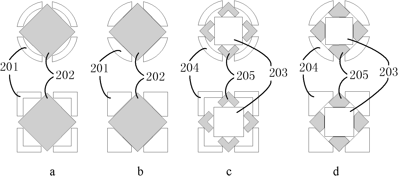
[0031] Specific embodiments of the present invention will be described in detail below in conjunction with the accompanying drawings. It should be noted that the specific embodiments discussed below are only specific embodiments in a specific environment, and do not limit the scope of the present invention. In order to better illustrate the structural characteristics of each layer of silicon chips in the laminated chip of the present invention, all silicon chips in the accompanying drawings are thinned. , The chip is temporarily bonded to the glass, thinned, permanently bonded to the silicon chip, and debonded from the glass. The present invention can be used on other semiconductor chips. The surrounding structures and micro-bumps shown are preferably square and circular, but can also be in any other shape. In addition, the dimensions in the embodiments are for better description of the invention. Not actual scale. The bonding between the metal micro-bumps in the present inv...
PUM
 Abstract
Description
Claims
Application Information