P-type MOS (Metal Oxide Semiconductor) memory cell
A storage unit and memory technology, applied in electrical components, transistors, electric solid state devices, etc., can solve the problems of increasing the size of the storage unit and affecting the performance of the storage unit.
- Summary
- Abstract
- Description
- Claims
- Application Information
AI Technical Summary
Problems solved by technology
Method used
Image

Examples
Embodiment Construction
[0030] In order to make the content of the present invention clearer and easier to understand, the content of the present invention will be described in detail below in conjunction with specific embodiments and accompanying drawings.
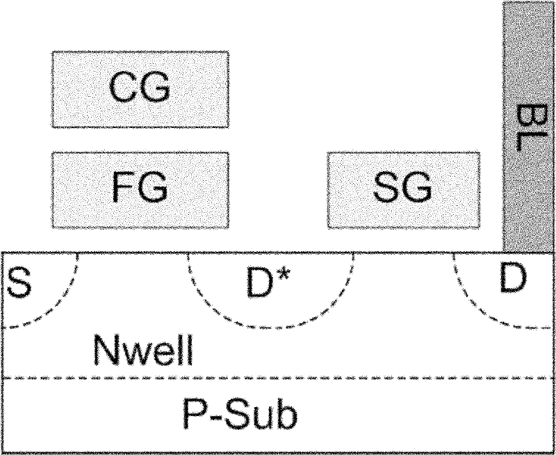
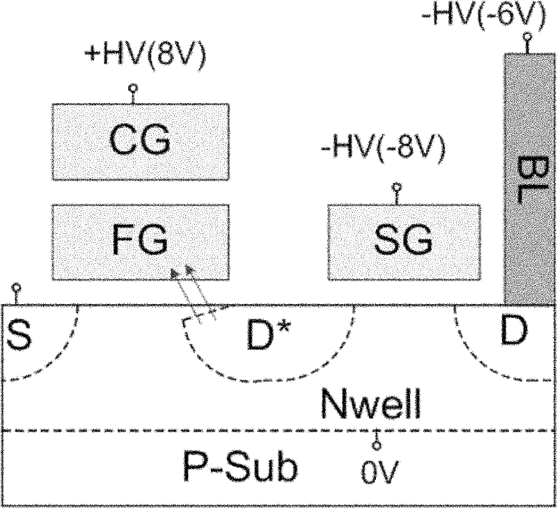
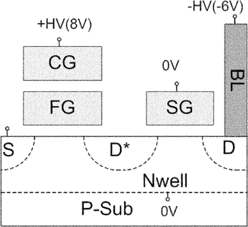
[0031] Figure 6 A schematic diagram showing the structure of a P-type memory cell according to an embodiment of the present invention.
[0032] Figure 6 The illustrated P-type MOS memory cell includes a source active region S, a gate active region, and a drain active region D arranged on a substrate P-Sub. The select gate SG, the control gate CG, and the floating gate FG are arranged above the gate active region, wherein the floating gate FG is arranged below the control gate CG. Wherein in the horizontal direction from the source active region S to the drain active region D, the select gate SG and the floating gate FG are sequentially arranged, and the control gate CG is in a floating position in the vertical direction (perpendicular to the...
PUM
 Abstract
Description
Claims
Application Information
 - R&D
- Intellectual Property
- Life Sciences
- Materials
- Tech Scout
- Unparalleled Data Quality
- Higher Quality Content
- 60% Fewer Hallucinations
Browse by: Latest US Patents, China's latest patents, Technical Efficacy Thesaurus, Application Domain, Technology Topic, Popular Technical Reports.
© 2025 PatSnap. All rights reserved.Legal|Privacy policy|Modern Slavery Act Transparency Statement|Sitemap|About US| Contact US: help@patsnap.com