Photon imaging system for detecting defects in photovoltaic devices, and method thereof

A photovoltaic device and defect technology, applied in photovoltaic system monitoring, measurement device, optical testing defect/defect and other directions, can solve the problems of failure to provide solar module reliability, light source consumption of large power, etc.

Inactive Publication Date: 2011-09-14
GENERAL ELECTRIC CO
View PDF4 Cites 7 Cited by
  • Summary
  • Abstract
  • Description
  • Claims
  • Application Information

AI Technical Summary

Problems solved by technology

This conventional technique provides information related to the power conversion efficiency of the solar module, but does not provide any information related to the reliability of the solar module
In addition, the operation of the light source consumes a large amount of power

Method used


Image

  • Photon imaging system for detecting defects in photovoltaic devices, and method thereof
  • Photon imaging system for detecting defects in photovoltaic devices, and method thereof
  • Photon imaging system for detecting defects in photovoltaic devices, and method thereof

Examples


Embodiment Construction

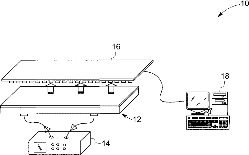
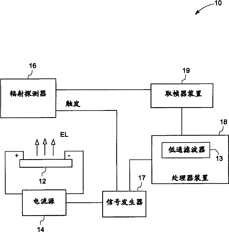
[0018] As discussed in detail below, embodiments of the present technology provide a diagnostic method for determining at least one defect in one or more photovoltaic devices, such as thin film photovoltaic modules. The method includes providing current to at least one photovoltaic device via a current source, and detecting emitted photon radiation from the at least one photovoltaic device via a radiation detector. The method also includes outputting a signal corresponding to the detected emitted photon radiation from the radiation detector to processor means, and processing the signal corresponding to the detected emitted photon radiation via the processor means to generate one or more binary dimensional photon image. The method also includes analyzing the one or more two-dimensional photonic images to determine at least one defect in at least one photovoltaic device. According to a specific embodiment, a diagnostic system for determining at least one defect in one or more p...


PUM


Abstract

A method includes supplying current to at least one photovoltaic device (12) via a current source (14) and detecting emitted photon radiations from the at least one photovoltaic device (12) via a radiation detector (16). The method also includes outputting a signal corresponding to the detected emitted photon radiations from the radiation detector (16) to a processor device (18), and processing the signal corresponding to the detected emitted photon radiations via the processor device (18) to generate one or more two-dimensional photon images. The method further includes analyzing the one or more two-dimensional photon images to determine at least one defect in the at least one photovoltaic device (12).

Description

technical field [0001] The present invention relates generally to photovoltaic devices, and more particularly to imaging systems and methods for detecting defects in photovoltaic cells, modules. Background technique [0002] Solar energy is considered an alternative energy source to other forms of energy. Solar energy conversion systems are used to convert solar energy into electrical energy. Solar energy conversion systems typically include photovoltaic modules, photovoltaic cells or solar cells that convert solar energy into electrical energy for direct use or for storage and later use. The conversion of solar energy to electrical energy involves: receiving light, such as sunlight, at the solar cell; absorbing sunlight into the solar cell; generating and separating positive and negative charges, thereby creating a voltage in the solar cell; Collect and transfer charge. [0003] In a solar module manufacturing line, it is helpful to identify local defects, hot spots, etc...

Claims


Application Information

Patent Timeline
Patent Type & Authority Applications(China)
IPC IPC(8): G01N21/88
CPCG01R31/2605G01N21/9505G01R31/308G01N21/66H02S50/10Y02E10/50
Inventor F·R·阿迈德O·苏利马K·R·纳加卡赵日安J·W·布雷
Owner GENERAL ELECTRIC CO
Why Eureka
Try Eureka