
Light-emitting diode packaging structure

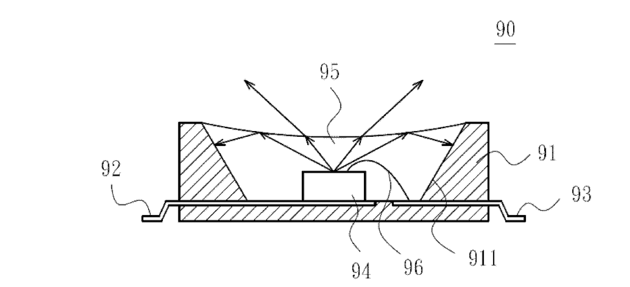
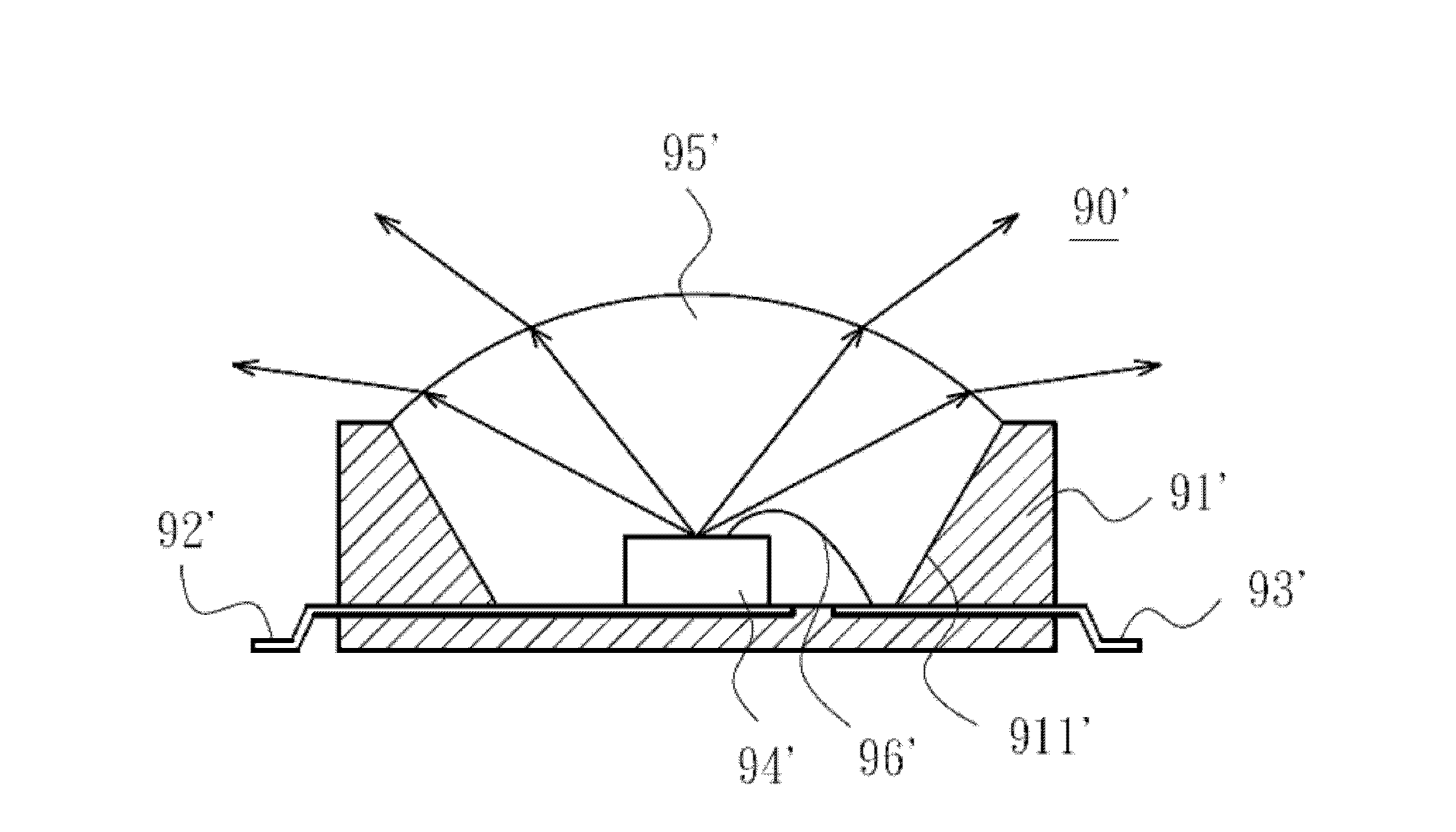
A technology for light-emitting diodes and structures, applied in electrical components, electrical solid-state devices, circuits, etc., can solve problems such as increasing the production cost of the light-transmitting packaging portion 95', unfavorable for light-emitting diode packaging structures SMT or other manufacturing processes, etc.

Inactive Publication Date: 2011-09-14
SHENZHEN CHINA STAR OPTOELECTRONICS TECH CO LTD
View PDF7 Cites 4 Cited by
  • Summary
  • Abstract
  • Description
  • Claims
  • Application Information

AI Technical Summary

Problems solved by technology

However, this will increase the manufacturing cost of the transparent encapsulation part 95'
Moreover, since the light-transmitting encapsulation part 95' protrudes from the housing 91', it is not conducive to the subsequent SMT or other manufacturing processes of the LED encapsulation structure 90'.

Method used


Image

  • Light-emitting diode packaging structure
  • Light-emitting diode packaging structure
  • Light-emitting diode packaging structure

Examples


Embodiment Construction

[0036] In order to make the above objects, features and advantages of the present invention more comprehensible, preferred embodiments of the present invention will be described in detail below together with the accompanying drawings. Wherein, in order to show the main part of the LED package structure more clearly, the three-dimensional schematic diagrams in the accompanying drawings of the present invention show the main features in a simplified manner.

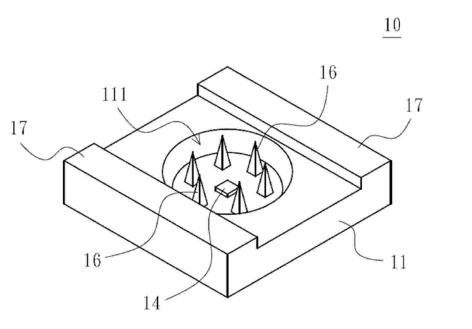
[0037] Please also refer to Figure 3A and Figure 3B , Figure 3A A three-dimensional schematic diagram of the housing and the LED chip of the first embodiment of the LED packaging structure of the present invention; Figure 3B It is a cross-sectional view of the first embodiment of the light emitting diode packaging structure of the present invention. The LED packaging structure 10 includes: a casing 11 , a first electrode sheet 12 , a second electrode sheet 13 , an LED chip 14 and a light-transmitting packaging portio...


PUM


Abstract

The invention discloses a light-emitting diode packaging structure comprising a shell, a light-emitting diode chip and a light-transmitting packaging part, wherein the shell is provided with a concave part and a plurality of projecting parts; the light-emitting diode chip is arranged in the concave part and covers the light-transmitting packaging part in the concave part; and the plurality of projecting parts are arranged in the concave part or at the edge of the shell. The light-emitting diode packaging structure enables the surface of the light-transmitting packaging part to be rugged through the plurality of projecting parts, thus increasing the diffusion angle of the light rays and improve the light producing efficiency of the light rays.

Description

【Technical field】 [0001] The present invention relates to a light-emitting diode packaging structure, in particular to a light-emitting diode packaging structure in which a plurality of protrusions are provided to make the surface of the light-transmitting packaging part into an uneven shape. 【Background technique】 [0002] Liquid crystal display (liquid crystal display, LCD) is a flat panel display device (flat panel display, FPD) that uses the characteristics of liquid crystal materials to display images. Power consumption and other advantages have become mainstream products in the entire consumer market. However, the liquid crystal material of the liquid crystal display cannot emit light on its own, and an external light source must be provided. Therefore, a backlight module needs to be provided in the liquid crystal display to provide the required light source. [0003] Generally speaking, backlight modules can be divided into two types: side-type backlight modules and ...

Claims


Application Information

Patent Timeline
Patent Type & Authority Applications(China)
IPC IPC(8): H01L33/48H01L33/58
CPCH01L33/60H01L33/54H01L2224/48091H01L2224/48247
Inventor 张光耀郑巍巍
Owner SHENZHEN CHINA STAR OPTOELECTRONICS TECH CO LTD
Learn More