Semi-precharging dynamic circuit

A dynamic circuit and pre-charging technology, applied in multiple input and output pulse circuits, etc., can solve the problems of voltage failure, increase DYN time, etc., and achieve the effect of eliminating DC power consumption

Inactive Publication Date: 2011-09-14
PEKING UNIV
View PDF5 Cites 0 Cited by
  • Summary
  • Abstract
  • Description
  • Claims
  • Application Information

AI Technical Summary

Problems solved by technology

[0012] 3. In image 3 In the comparator implemented by a simple differential amplifier, when Vin is greater than Vref, OUT- will become low level, making M4 open, and the setting of Vref will also open M2 to a certain extent, causing DC power consumption from M4 to M2
This is because the final voltage of OUT+ is the result of the voltage division between M4 and M2. If Vref is too small, the voltage of OUT+ cannot drop to a low level.
And Vref is required to be slightly smaller than the voltage that DYN is precharged to, so the only way to increase the precharge voltage is to make it greater than V DD / 2 to make the whole circuit work properly, which increases the time for DYN to be pulled down to GND

Method used


Image

  • Semi-precharging dynamic circuit
  • Semi-precharging dynamic circuit
  • Semi-precharging dynamic circuit

Examples


Embodiment Construction

[0037] The specific implementation manners of the present invention will be further described in detail below in conjunction with the accompanying drawings and embodiments. The following examples are used to illustrate the present invention, but are not intended to limit the scope of the present invention.

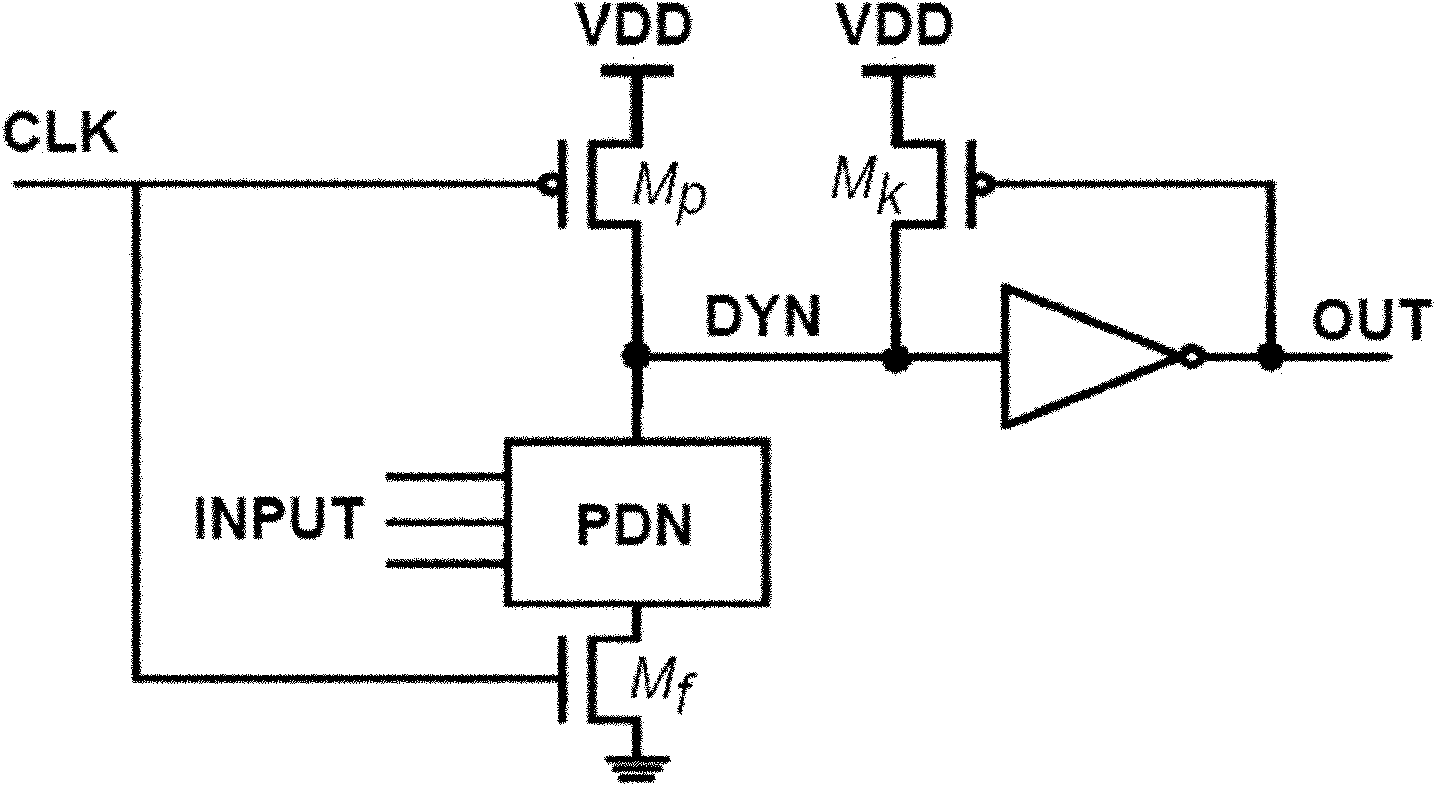
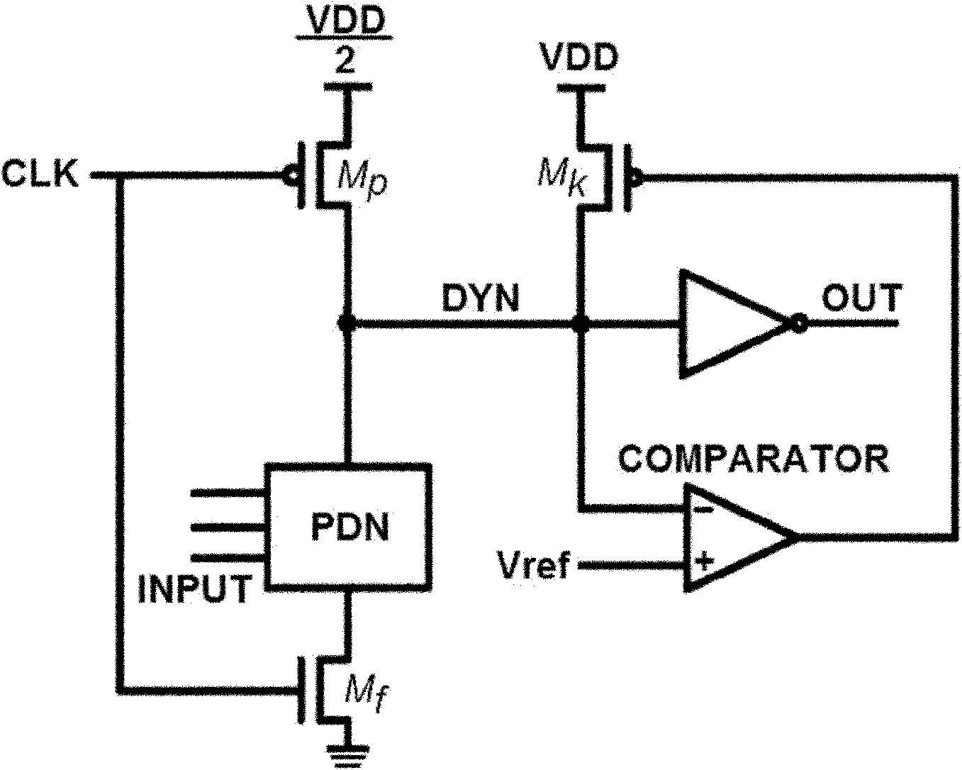
[0038] Such as Figure 4 As shown, it is a structural diagram of a semi-precharge dynamic circuit according to an embodiment of the present invention. The semi-precharge dynamic circuit includes: a first precharge tube Mp1, a pull-down logic network PDN, a hold tube Mk, an NMOS tube Mf, and an output inversion device and a comparator, the drain end of the first prefill pipe Mp1 is connected to the drain end of Mk to form a dynamic node DYN, one end of the PDN is connected to the DYN, and the other end is connected to the drain end of the Mf, and the comparator The negative input terminal of Mk is connected to DYN, the gate of Mk is connected to the output terminal of the ...


PUM


Abstract

The invention discloses a semi-precharging dynamic circuit, which comprises a first precharging transistor Mp1, a pull down net PDN, maintaining transistors Mk and Mf, an output inverter, a comparator and a transmission transistor, wherein the drain of the first precharging transistor Mp1 is connected with the drain of the Mk to form a dynamic node DYN; one end of the PDN is connected with the DYN, and the other end of the PDN is connected with the drain of the Mf; the negative input end of the comparator is connected with the DYN; the gate of the Mk is connected with the output end of the comparator; the gates of the Mp1 and the Mf are both connected with a pulse CLK; the N-channel metal oxide semiconductor (NMOS) transmission transistor Mg and a second precharging transistor Mp2 are arranged between the output inverter and the DYN; the DYN is connected with the input end of the output inverter by the transmission transistor Mg; the drain of the Mp2 is connected with the transmission transistor Mg; and the gates of the Mp2 and the Mg are both connected with the pulse CLK. The semi-precharging dynamic circuit eliminates the DC power consumption of the output inverter on the premise of ensuring noise cancellation, realizes real semi-precharging, and voids a DC path from a power supply VDD to the power supply VDD/2.

Description

technical field [0001] The invention relates to the technical field of dynamic circuits in CMOS circuits, in particular to a semi-precharge dynamic circuit. Background technique [0002] The function realization of CMOS circuit can be completed by static circuit or dynamic circuit. Traditional CMOS static circuits suffer from inherent speed limitations due to the input signal driving both NMOS and PMOS transistors. The input signal of the CMOS dynamic circuit only needs to drive the NMOS (or PMOS) transistor, so it has great advantages over the CMOS static circuit in terms of speed and area. [0003] Traditional CMOS dynamic circuit structures such as figure 1 shown [1] , which mainly includes a pre-charge tube (Mp), a pull-down logic network (Pull Down Net (PDN)), a hold tube (Mk) and an output inverter. The delay of traditional CMOS dynamic circuits is mainly determined by the time from the start of the evaluation stage to when DYN is pulled down to GND (if it needs to...

Claims


Application Information

Patent Timeline
Patent Type & Authority Applications(China)
IPC IPC(8): H03K5/22
Inventor 贾嵩孟庆龙杨凯王源张钢刚
Owner PEKING UNIV
Why Eureka
Try Eureka