
Fully balanced dual-port memory cell

A memory unit and channel technology, applied in the field of memory, can solve problems such as inconvenience, and achieve the effect of reducing development investment

Active Publication Date: 2013-03-27
TAIWAN SEMICON MFG CO LTD
View PDF3 Cites 0 Cited by
  • Summary
  • Abstract
  • Description
  • Claims
  • Application Information

AI Technical Summary

Problems solved by technology

[0005] It can be seen that the above-mentioned existing embedded static random access memory device obviously still has inconvenience and defects in structure and use, and needs to be further improved urgently.

Method used


Image

  • Fully balanced dual-port memory cell
  • Fully balanced dual-port memory cell
  • Fully balanced dual-port memory cell

Examples


Embodiment Construction

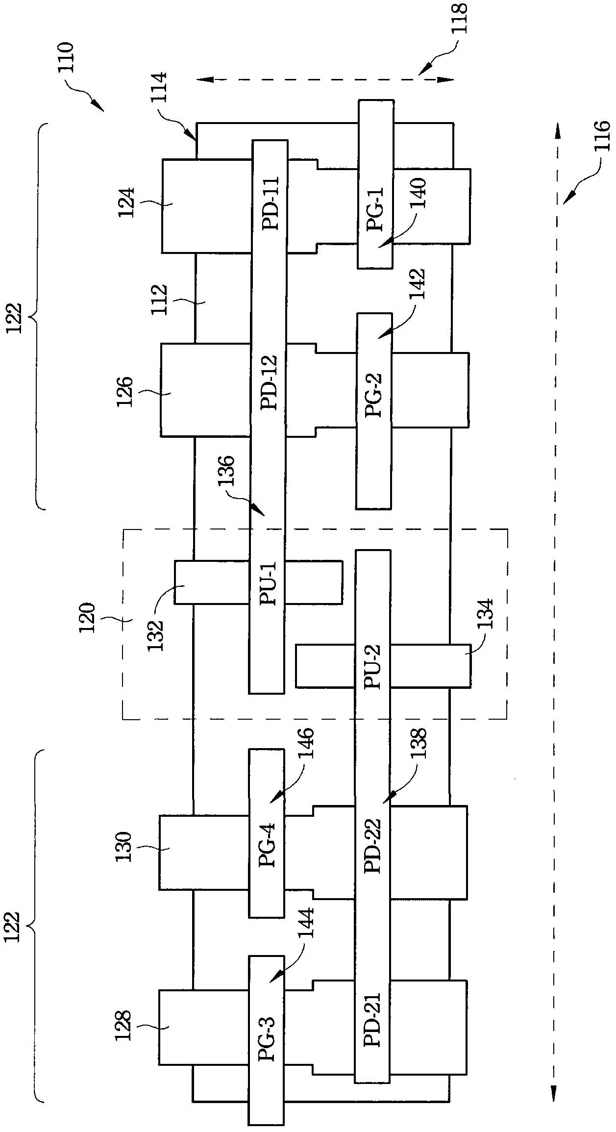
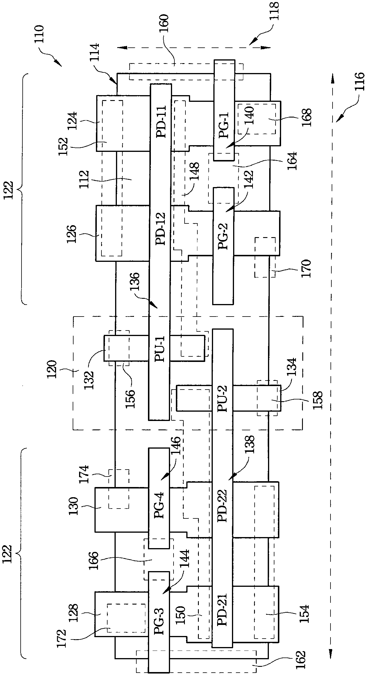
[0078] In order to further explain the technical means and effects that the present invention adopts to achieve the intended purpose of the invention, the specific implementation, structure and characteristics of the fully balanced dual-channel memory unit proposed according to the present invention will be described below in conjunction with the accompanying drawings and preferred embodiments. And its effect, detailed description is as follows.

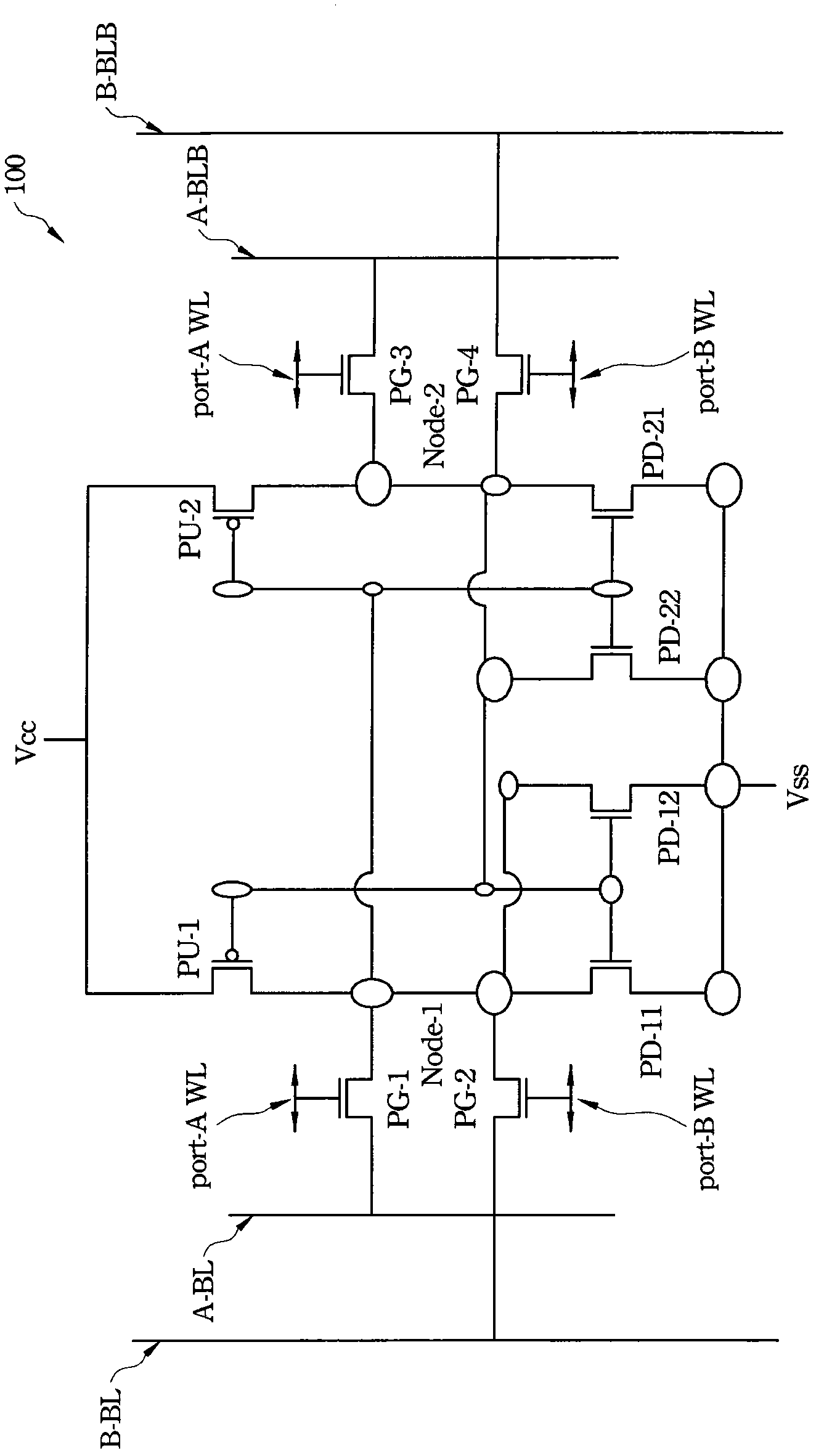
[0079] figure 1 It is a schematic diagram illustrating a dual-channel SRAM unit 100 according to an embodiment of the present invention. The dual-channel SRAM unit 100 includes a first inverter and a second inverter, and the first inverter and the second inverter are cross-coupled to each other. The first inverter includes a first pull-up device PU-1, a first pull-down device PD-11, and a second pull-down device PD-12. The first pull-up device PU-1 is formed by a P-type metal-oxide-semiconductor field-effect transistor (p-type met...


PUM


Abstract

The present disclosure provides a dual port static random access memory (SRAM) cell. The dual-port SRAM cell includes four sets of cascaded n-type metal-oxide-semiconductor field-effect transistors (NMOSFETs), each set of cascaded NMOSFETs having a pull-down device and a pass-gate device; and a first and second pull-up devices (PU1 and PU2) configured with the four pull-down devices to form two cross-coupled inverters, wherein two of the pass-gate devices are configured to form a first port and another two of the pass-gate devices are configured to form a second port.

Description

technical field [0001] The invention relates to a memory, in particular to a static random access memory unit. Background technique [0002] In deep sub-micron integrated circuit technology, embedded static random access memory devices have become the main storage unit in high-speed communication, image processing and single-chip system products. For example, dual-channel SRAM devices can allow parallel operations, such as simultaneous reading and writing or two simultaneous read operations in one cycle, so dual-channel SRAM devices are more efficient. Single-channel SRAM devices have higher bandwidth. In the advanced technology of embedded memory and system-on-a-chip products, the low loading and high-speed characteristics of the static random access memory cell structure are its important characteristics. Thin SRAM cell structure with short bit lines has better performance in terms of RC delay of the bit lines. [0003] However, the thin SRAM cell structure still encoun...

Claims


Application Information

Patent Timeline
Patent Type & Authority Patents(China)
IPC IPC(8): G11C11/412G11C11/419
CPCG11C11/413G11C11/412G11C8/16
Inventor 廖忠志谢志宏
Owner TAIWAN SEMICON MFG CO LTD
Learn More