Substrate structure and manufacturing method thereof

A manufacturing method and substrate technology, applied in semiconductor/solid-state device manufacturing, electrical components, electrical solid-state devices, etc., can solve the problem of low thermal resistance

Active Publication Date: 2011-09-21
IND TECH RES INST
View PDF3 Cites 10 Cited by
  • Summary
  • Abstract
  • Description
  • Claims
  • Application Information

AI Technical Summary

Problems solved by technology

[0005] Due to the incompatibility with flexible substrate materials and low thermal resistance, traditional release layer materials are not suitable for TFT processes

Method used


Image

  • Substrate structure and manufacturing method thereof
  • Substrate structure and manufacturing method thereof
  • Substrate structure and manufacturing method thereof

Examples


Embodiment 1

[0043] Fabrication of polyimide B1317-BAPPm(BB) / Topas(X=50, Y=50) / glass substrate structure

[0044] First, prepare Topas solutions with different solid content (1%, 3%, 6%, 7%, 8%). Afterwards, the Topas solution was coated on different glass support carriers to form a wet Topas film. The thickness of the wet Topas film is 30 μm, 60 μm, 90 μm, and 120 μm, respectively. After baking at 50°C for 5 minutes and 300°C for 1 hour, apply a polyimide substrate material (containing 1% adhesion promoter) on the Topas film. After baking again, perform a release test, and the results are shown in Table 1.

[0045] Table I

[0046] Topas solid content

Embodiment 2

[0048] Fabrication of polyimide B1317-BAPPm(BB) / Arton(X=50, Y=50, R=H) / glass substrate structure

[0049] First, prepare Arton solutions with different solid content (5%, 10%, 15%, 20%, 25%). Afterwards, the above-mentioned Arton solution was coated on different glass support carriers to form a wet Arton film. The thickness of the wet Arton film is 30 μm, 60 μm, 90 μm, and 120 μm, respectively. After baking at 50°C for 5 minutes and 300°C for 1 hour, apply a polyimide substrate material (containing 1% adhesion promoter) on the Arton film. After baking again, a release test was performed, and the results are shown in Table 2.

[0050] Table II

[0051] Arton solid content

Embodiment 3

[0053] The production of parylene release layer

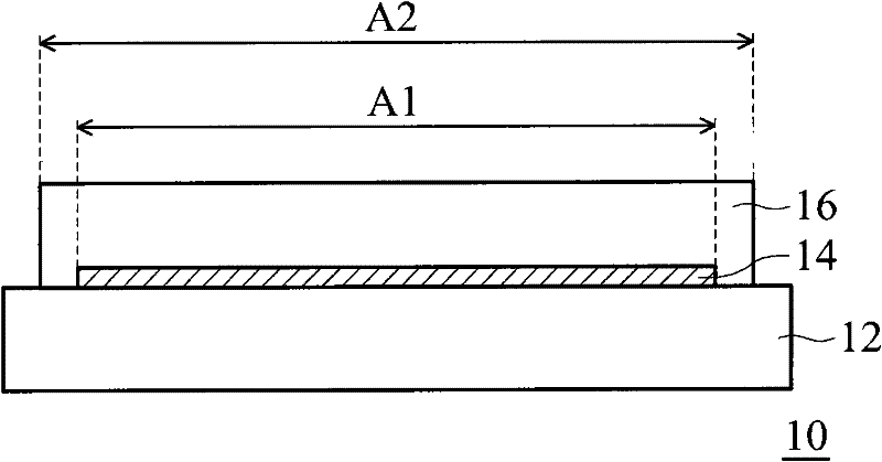
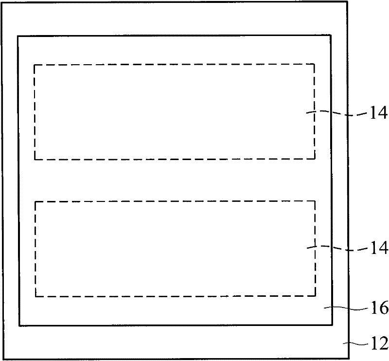
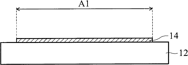
[0054] Put the parylene dimer (parylene dimer) into the thermal evaporation equipment, put the pre-washed glass (15cm*15cm) into the sample chamber, and cover the glass with a hollow (8cm*8cm) gasket After vacuuming, heat to 150°C to vaporize the precursor of parylene, and then heat to 650°C to crack the raft door and open the raft door to the sample chamber, and polymerize and deposit at room temperature without being covered by gaskets. In the glass area, an 8cm*8cm release film is formed.


PUM


Abstract

The invention provides a substrate structure applied to soft electronic elements. The substrate structure comprises a supporting carrier, a release layer which covers the supporting carrier by a first area, and a soft substrate which covers the release layer and the supporting carrier by a second area; the second area is larger than the first area; and the density of the soft substrate to the supporting carrier is larger than the density of the release layer to the supporting carrier. The invention also provides a manufacturing method of the substrate structure.

Description

Technical field [0001] The present invention relates to a substrate structure, in particular to a substrate structure applied to flexible electronic components and a manufacturing method thereof. Background technique [0002] Flexible displays have become the development trend of novel displays in the new era, and the development of active flexible displays is the mainstream trend. The world’s major R&D companies have moved from the current thick and fragile glass substrates to non-glass and lighter weight The development of flexible plastic substrate materials, and towards active full-color TFT display panels. Currently, there are three options for the development of active flexible display technologies: a-Si TFT, LPTSTFT and OTFT. The display medium includes EPD, ECD, LCD and EL. [0003] The choice of manufacturing method can be divided into two methods: batch type and roll to roll. If you choose batch type for TFT element manufacturing, you can use existing TFT equipment for m...

Claims


Application Information

Patent Timeline
Patent Type & Authority Applications(China)
IPC IPC(8): H01L27/12H01L21/78
Inventor 廖学一吕奇明苏俊玮
Owner IND TECH RES INST
Why Eureka
Try Eureka