Light-emitting devices and its forming method

A light-emitting unit, flat technology, applied to the structure of optical waveguide semiconductors, semiconductor devices, electrical components, etc., can solve the problems of increased cost and complexity, inability to improve light leakage efficiency, etc., to achieve low cost and increase the light output area. Effect

Active Publication Date: 2011-09-21
EPISTAR CORP
View PDF4 Cites 4 Cited by
  • Summary
  • Abstract
  • Description
  • Claims
  • Application Information

AI Technical Summary

Problems solved by technology

However, the above method increases the cost and complexity of the packaging substrate and the bonding process for connecting the light-emitting device chip to the packaging substrate.
In addition, the solutions using the above packaging substrates cannot improve their light-extraction efficiency.

Method used


Image

  • Light-emitting devices and its forming method
  • Light-emitting devices and its forming method
  • Light-emitting devices and its forming method

Examples


Embodiment Construction

[0038] Hereinafter, novel light emitting devices and methods of forming the same according to embodiments of the present invention will be described. The diagrams are shown at intermediate stages in the manufacturing process in the examples. It then discusses variations and operations of embodiments of the invention. In these different drawings and illustrated embodiments, the same reference numerals are used to represent the same elements.

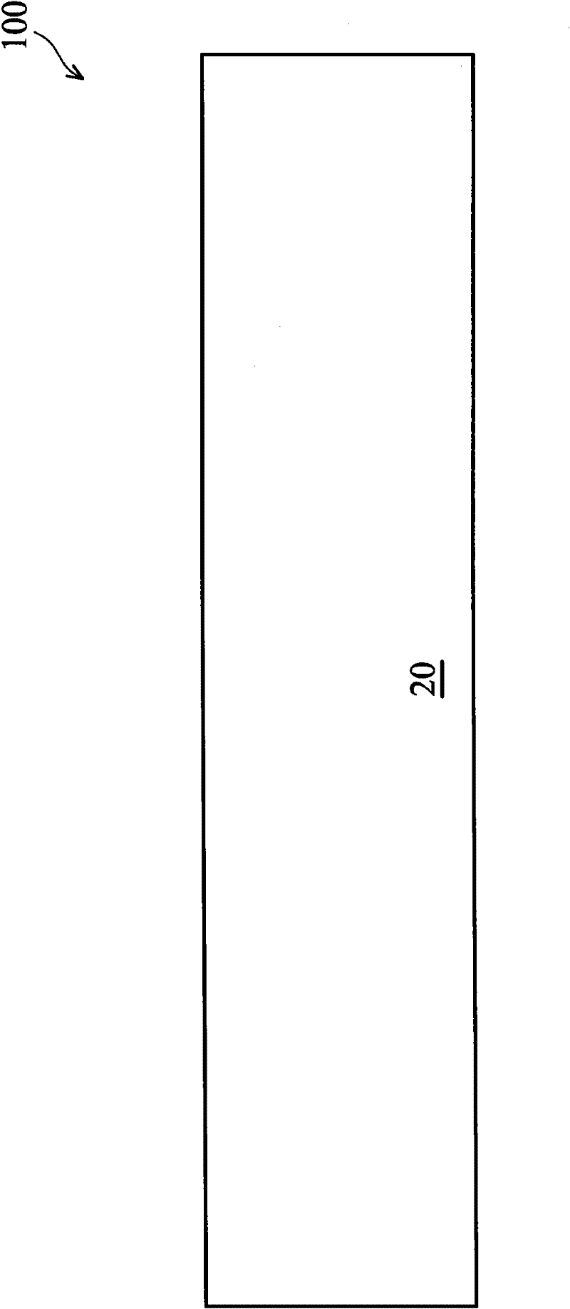
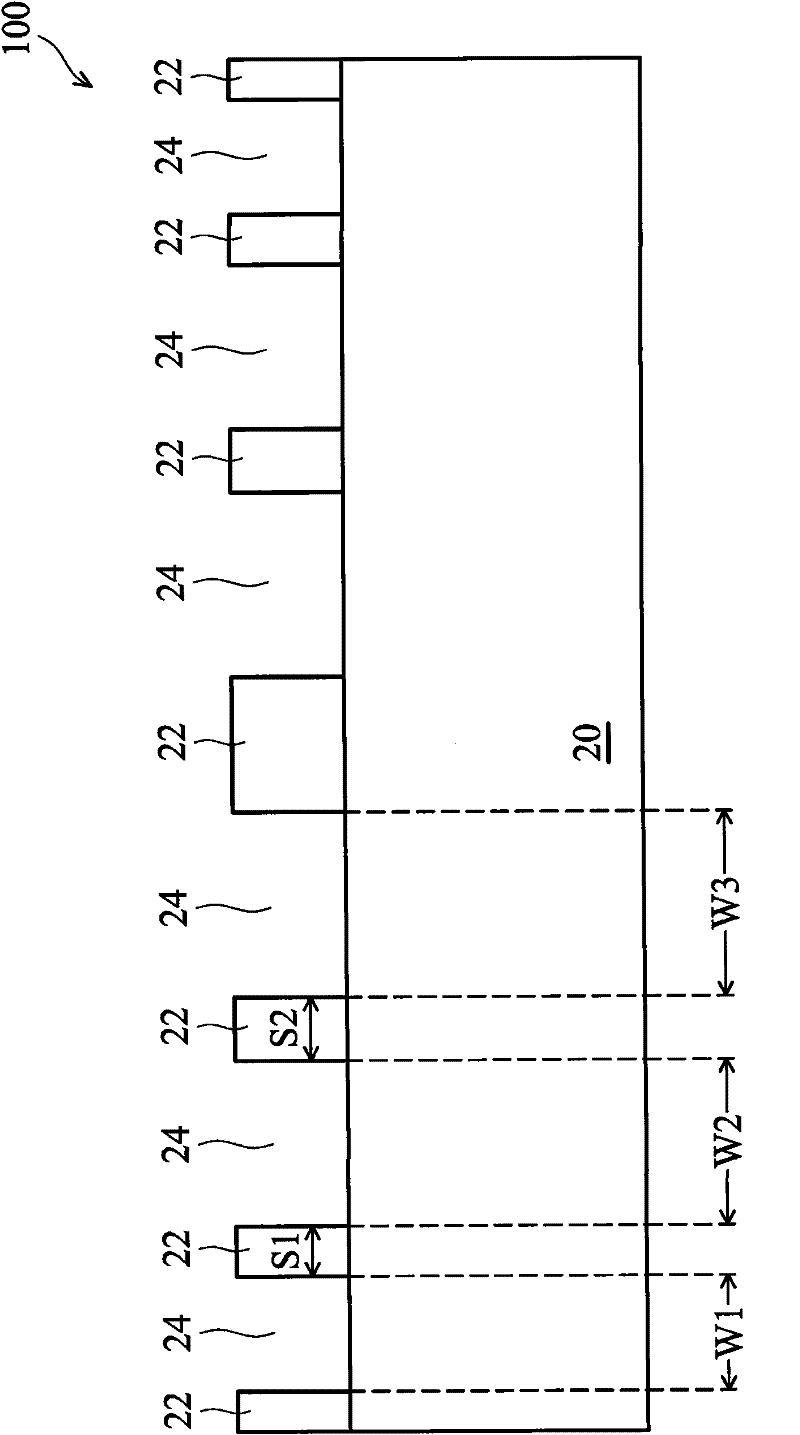
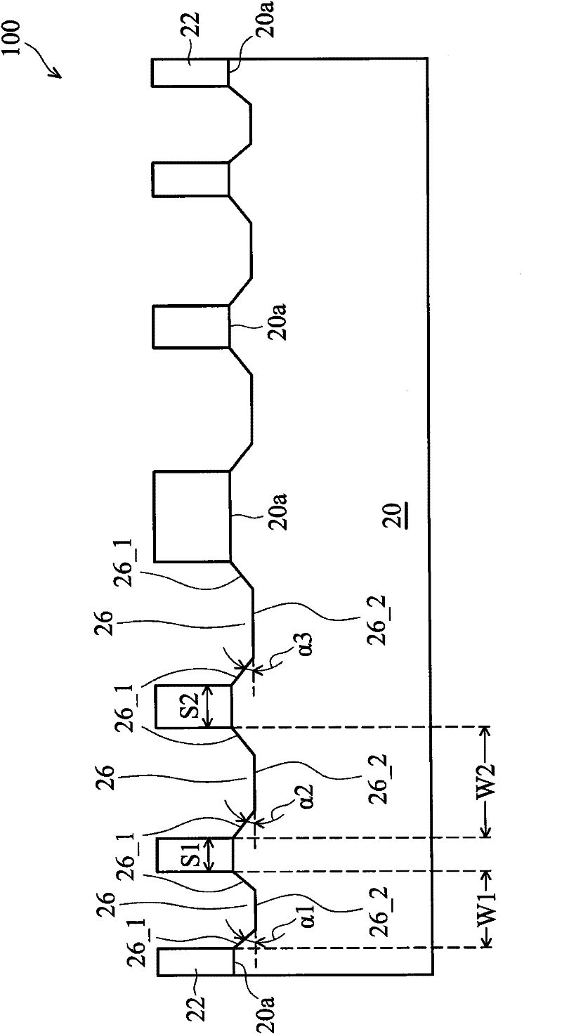
[0039] Please refer to figure 1 , first provide the chip 100 including the substrate 20 . Chip 100 may be a portion of an un-diced wafer comprising a plurality of identical chips. In one embodiment, the substrate 20 can be made of sapphire (sapphire, Al 2 o 3 ) formed. In other embodiments, the substrate 20 is a silicon-containing substrate, such as a silicon carbide substrate or a silicon substrate. In other embodiments, the substrate 20 includes compound semiconductor materials of group III and / or group V elements, or includes w...


PUM


Abstract

The invention relates to a light-emitting device and its forming method. The light-emitting device comprises: a textured substrate comprising a first groove extending from a top of the textured substrate into the textured substrate, wherein the groove comprises a first side wall and a bottom. The light-emitting device is arranged on the textured substrate and composed of an active layer and a first, second covering layers with opposite electrical properties, wherein the active layer comprises a first portion in parallel to a first side wall and a second portion in parallel to the bottom of the groove and the first covering layer and the second covering layer are on the opposite sides of the active layer. The light output area is increased and the total amount of the emitting light of a single chip is also increased.

Description

technical field [0001] The present invention relates to a light-emitting device (light-emitting device, LED), and in particular to a method for manufacturing a light-emitting device with textured active layers and a formation structure thereof. Background technique [0002] Light-emitting devices (LEDs), such as light-emitting diodes or laser diodes, have been widely used in many applications. As known by those skilled in the art, a light emitting device may include a semiconductor light emitting device having a plurality of semiconductor layers formed on a substrate. The above substrate can be formed of materials such as gallium arsenide, gallium phosphide, alloys of the above materials, silicon carbide and / or sapphire. The continued development of light emitting devices has resulted in highly efficient and robust light sources covering the visible spectrum and beyond. As such, the use of solid-state devices with their potentially long lifetimes will facilitate their use ...

Claims


Application Information

Patent Timeline
Patent Type & Authority Applications(China)
IPC IPC(8): H01L33/20H01L33/24H01S5/24
CPCH01L33/24H01L33/22H01L33/04
Inventor 黄信杰
Owner EPISTAR CORP
Why Eureka
Try Eureka