

Pixels of multi-domain vertical alignment liquid crystal displays
A liquid crystal display, vertical alignment technology, applied in static indicators, instruments, nonlinear optics, etc., can solve the problems of expensive manufacturing, high cost, and reduced brightness of liquid crystal displays
- Summary
- Abstract
- Description
- Claims
- Application Information
AI Technical Summary
Problems solved by technology
Method used
Image


Examples
Embodiment Construction
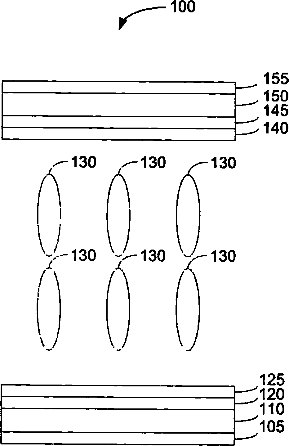
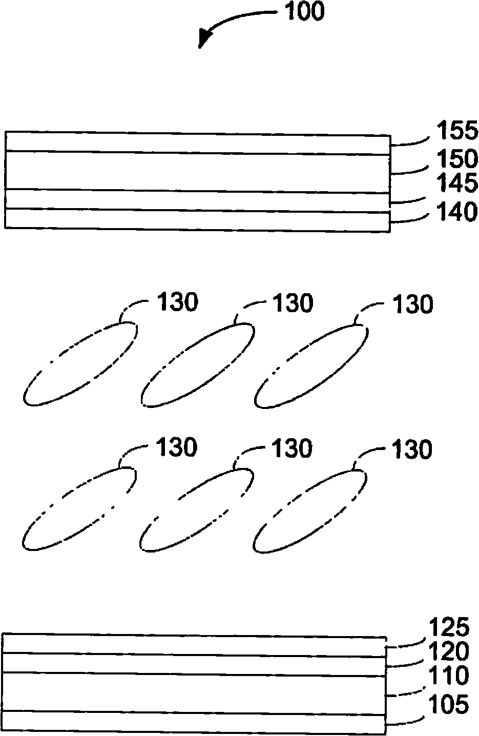
[0154] As mentioned above, conventional multi-domain vertical alignment liquid crystal displays are very expensive to manufacture because of the use of physical features such as protrusions or ITO gaps to create multiple domains per pixel. However, according to the method of the present invention, the multi-domain vertical alignment liquid crystal display uses discrete electric fields to generate multiple domains, and does not require the use of physical features (such as protrusions or ITO gaps) on the substrate. Furthermore, since no physical characteristics are required, the difficulty of calibrating the physical characteristics of the upper and lower substrates can also be eliminated. Therefore, compared with the traditional multi-domain vertical alignment liquid crystal display, the multi-domain vertical alignment liquid crystal display according to the present invention has a higher yield and is cheaper to manufacture.
[0155] Please refer to Figure 3a and Figure 3b...
PUM
 Abstract
Description
Claims
Application Information