Integrated circuit device and packaging assembly

A technology of integrated circuits and conductive pillars, applied in the field of bump structures, can solve the problems of high manufacturing cost, interface peeling, and manufacturing cost attachment situation.

Inactive Publication Date: 2011-09-28
TAIWAN SEMICON MFG CO LTD
View PDF7 Cites 12 Cited by
  • Summary
  • Abstract
  • Description
  • Claims
  • Application Information

AI Technical Summary

Problems solved by technology

Therefore, a sidewall protection layer is required to avoid oxidation of copper, but known methods for fabricating copper pillar sidewalls suffer from high manufacturing cost and interface peeling.
At present, the immersion tin process is used to form a tin layer on the sidewall of the copper pillar. However, the above-mentioned technology still has problems related to manufacturing cost, adhesion between tin and primer, and solder wetting on the sidewall. , the above problems are a major challenge for the fine-pitch packaging technology in the new generation of chips

Method used


Image

  • Integrated circuit device and packaging assembly
  • Integrated circuit device and packaging assembly
  • Integrated circuit device and packaging assembly

Examples


Embodiment Construction

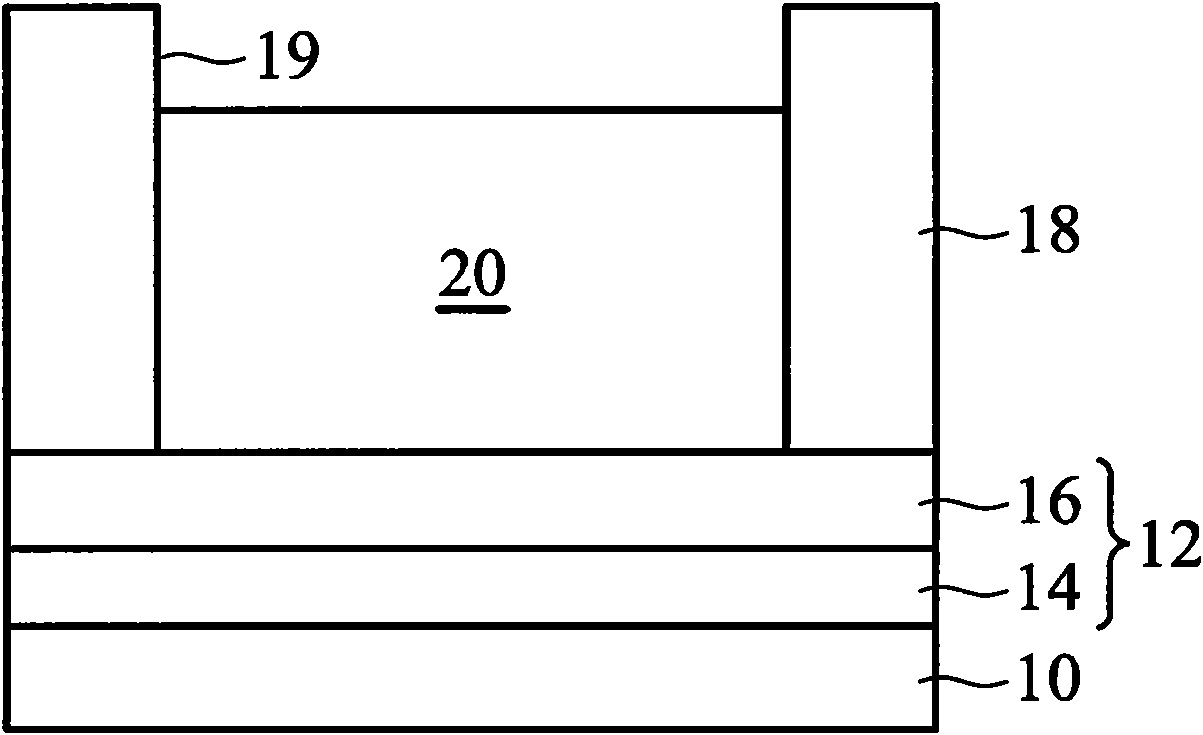
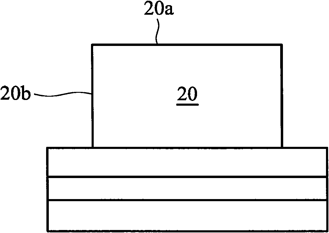
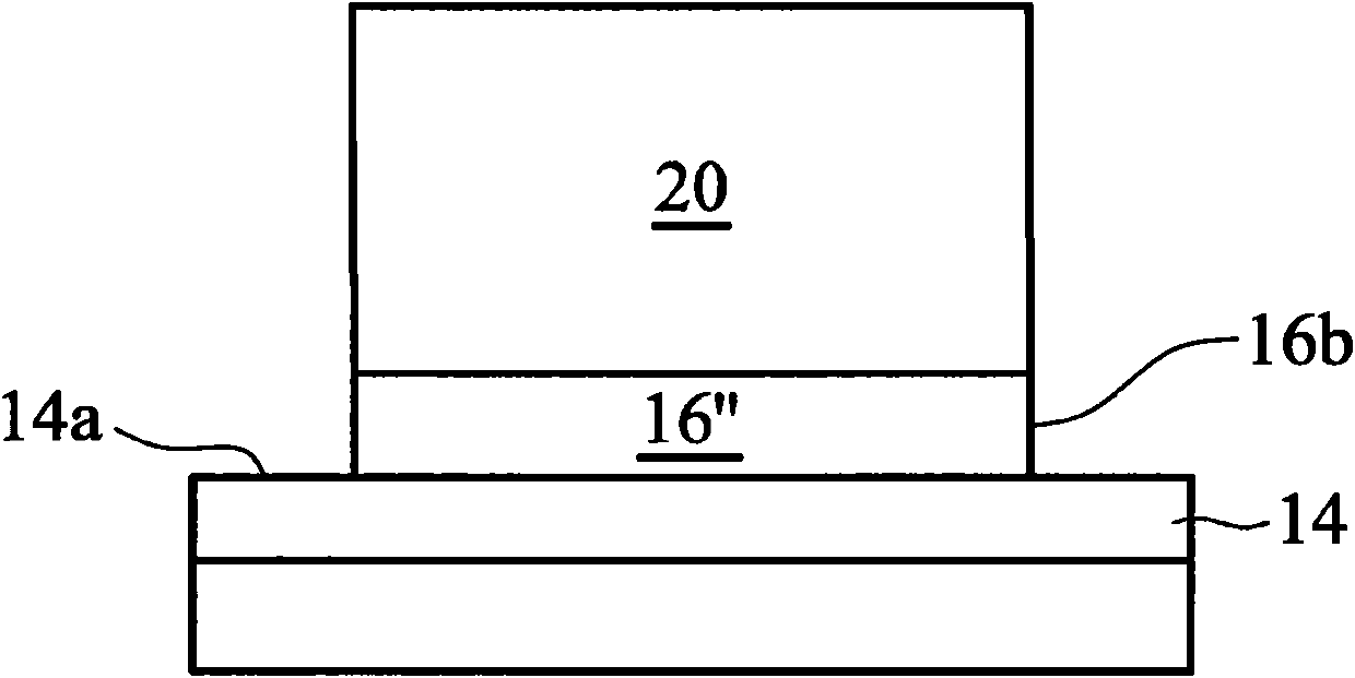
[0052] The present invention provides several embodiments of the sidewall protection process applicable to the copper pillar bump technology. Or the protective structure of one of the multiple non-metallic material film layers such as the combination of the above material film layers. The term "Cu pillar bump" used hereinafter refers to a bump structure including a conductive pillar (a pillar or a support base) formed of copper or copper alloy. The copper stud bumps can be directly applied on the conductive pads of a semiconductor chip or a redistribution layer of a flip-chip assembly or in other similar applications.

[0053] Examples and embodiments of the present invention are explained in detail below with reference to the corresponding drawings. Where possible, the same reference numbers have been used throughout the drawings and description to refer to the same or similar components. In the drawings, for the purpose of clarity and convenience, the shapes or thicknesses...


PUM


Abstract

The invention discloses an integrated circuit device and a packaging assembly. The integrated circuit device comprises a semiconductor substrate; a first bump bottom metal layer formed on the semiconductor substrate; a second bump bottom metal layer formed on the first bump bottom metal layer and equipped with a side surface; a conductive column formed on the second bump metal layer and equipped with a side surface and a top surface and a protection structure formed on the side surfaces of the conductive column and the second bump bottom metal layer. The protective structure is made of non-metallic material and the conductive column is formed of a copper-containing layer. The protection technology for the sidewall of copper stud bumps is adopted by the invention, wherein the side surface of a copper stud bump is equipped with a protective structure formed by at least one non-metallic material film layer selected from a dielectric material layer, a polymer layer or the combination of the above layers. According to the invention, the stress force on a substrate can be adjusted and the solder wetting condition of surrounding copper studs is avoided.

Description

technical field [0001] The present invention relates to integrated circuit fabrication, and more particularly to bump structures used in integrated circuit devices. Background technique [0002] Today's integrated circuits are formed from millions of devices such as transistors or capacitors. These devices are initially separated, but are then interconnected with each other to form a functional circuit. The interconnection structure generally includes horizontal interconnection such as metal wires (connection lines) and vertical interconnection such as vias and contacts. These interconnect scenarios are increasingly setting the performance and density limits of today's integrated circuits. On top of the interconnect structure, bond pads are formed and expose the surface of each chip. The pads can be used to form an electrical connection between the chip and the substrate or another chip. The bonding pads can be used for bonding situations such as wire bonding or flip-chi...

Claims


Application Information

Patent Timeline
Patent Type & Authority Applications(China)
IPC IPC(8): H01L23/00
CPCH01L2224/13655H01L2924/01049H01L2224/1182H01L2224/05647H01L24/11H01L2224/81411H01L2924/01032H01L2224/13664H01L24/05H01L2224/05181H01L2224/81416H01L2924/01078H01L2224/11827H01L2224/13562H01L24/16H01L2224/13565H01L2224/81455H01L2224/0361H01L24/13H01L2924/01024H01L2924/01005H01L2224/05166H01L2224/13147H01L2924/01013H01L2924/01322H01L24/03H01L2224/05187H01L2224/0345H01L2224/1146H01L2224/11901H01L2224/05024H01L2924/01012H01L2224/13564H01L2224/1369H01L2224/81024H01L2224/13639H01L2224/13611H01L2224/10126H01L2224/0569H01L2224/814H01L2224/03614H01L2224/11464H01L2224/13644H01L2224/11462H01L2924/0105H01L2224/03912H01L2224/1132H01L2224/81191H01L2924/01025H01L2224/81447H01L2224/11849H01L2224/1145H01L2924/01047H01L2224/1147H01L2224/05578H01L2924/01006H01L2224/81815H01L2924/01079H01L2924/01073H01L2224/81439H01L2224/81413H01L2924/01038H01L2224/05073H01L2224/13647H01L2224/11452H01L2924/0103H01L2924/01082H01L2224/13099H01L2924/13091H01L2924/0104H01L2224/13582H01L2224/023H01L2924/014H01L2224/13609H01L2224/13583H01L2924/01023H01L2224/0401H01L2924/01029H01L2224/11912H01L2224/03901H01L2924/01019H01L2924/01033H01L2924/01075H01L24/81H01L2924/1305H01L2924/04941H01L2924/04953H01L2924/01028H01L2924/01022H01L2924/01007H01L2924/01014H01L2924/01015H01L2924/01046H01L2924/01083H01L2924/01051H01L2924/00H01L2924/14H01L2224/05016H01L2924/206H01L2924/2064H01L2924/20641H01L2924/20642H01L2224/13561H01L2224/16238H01L2224/11614H01L21/76885
Inventor 黄见翎吴逸文王俊杰刘重希
Owner TAIWAN SEMICON MFG CO LTD
Why Eureka
Try Eureka