Supercharge Your Innovation With Domain-Expert AI Agents!

Integrated circuit 3D memory array and manufacturing method

A manufacturing method and memory technology, applied in semiconductor/solid-state device manufacturing, circuits, electric solid-state devices, etc., can solve problems such as high manufacturing cost and limited use

Inactive Publication Date: 2011-10-12
MACRONIX INT CO LTD
View PDF10 Cites 8 Cited by
  • Summary
  • Abstract
  • Description
  • Claims
  • Application Information

AI Technical Summary

Problems solved by technology

Thus, although the use of 3D arrays has the advantage of achieving higher densities, higher manufacturing costs limit the use of this technology

Method used


Image

  • Integrated circuit 3D memory array and manufacturing method
  • Integrated circuit 3D memory array and manufacturing method
  • Integrated circuit 3D memory array and manufacturing method

Examples


Embodiment Construction

[0095] refer to Figures 1 to 16 , provides a detailed description of embodiments of the invention.

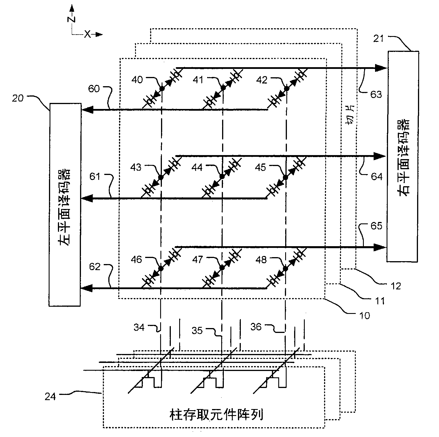
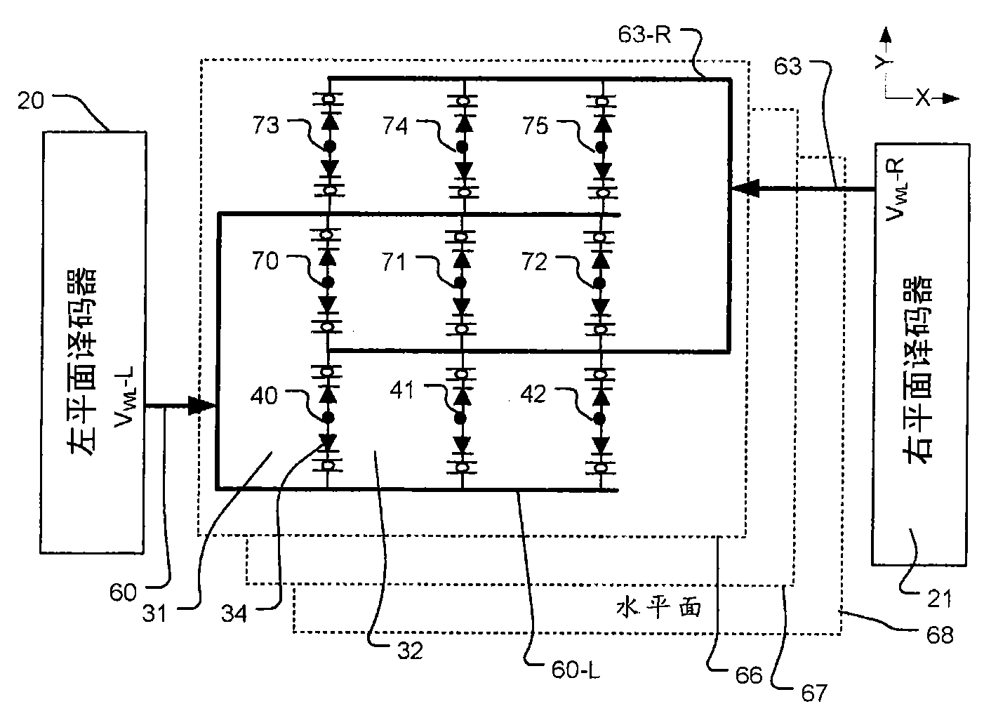
[0096] figure 1 Is a schematic diagram of a 3D memory element showing "slices" 10 , 11 , 12 placed in the X-Z plane of the 3D structure. In the schematic diagram shown, there are nine two-cell cell structures 40 to 48, each cell structure has two memory cells with separate programmable components and left and right gates . Each slice of an embodiment of a 3D memory element may include many dual memory cell cell structures. The elements include an array of memory cells arranged for left and right decoding using a left plane decoder 20 , a right plane decoder 21 and an array of pillar access elements 24 . The semiconductor pillars of the dual memory cell structure are coupled in the Z-direction columns (e.g. 40, 43, 46) to the access elements in the pillar access element array 24 via semiconductor pillars (e.g. 34), such as integrated circuit substrates under the structure. ...


PUM


Abstract

The invention discloses an integrated circuit 3D memory array and a manufacturing method and relates to a 3D memory element based on an array of conductive pillars and a plurality of patterned conductor planes and a manufacturing method. The 3D memory device is based on an array of conductive pillars and a plurality of patterned conductor planes including left side and right side conductors adjacent the conductive pillars at left side and right side interface regions. Memory elements in the left side and right side interface regions comprise a programmable element and a rectifier. The conductive pillars can be selected using two-dimensional decoding, and the left side and right side conductors in the plurality of planes can be selected using decoding on a third dimension, combined with left and right side selection.

Description

technical field [0001] The present invention relates to a high density memory device, and more particularly to a memory device in which multiple planes of memory cells are arranged to provide a three-dimensional 3D array. Background technique [0002] As the critical dimensions of components in integrated circuits shrink to the limits of general memory cell technology, designers have paid attention to techniques for stacking multiple planes of memory cells to achieve larger storage capacities and lower cost per bit . For example, "512-Mb PROM With a Three-Dimensional Array of Diode / Anti-fuse Memory Cells," IEEE Journal of Solid State Circuits, Vol. Cross-point array technology of silk memory. In the design described by Johnson et al., multiple layers of wordlines and bitlines are provided, with memory elements located at intersections. The memory element includes a p+ polysilicon anode connected to a word line, and an n- polysilicon cathode connected to a bit line, the an...

Claims


Application Information

Patent Timeline
Patent Type & Authority Applications(China)
IPC IPC(8): H01L23/525H01L21/768
CPCH01L27/0688H10B20/25
Inventor 龙翔澜
Owner MACRONIX INT CO LTD
Features
  • R&D
  • Intellectual Property
  • Life Sciences
  • Materials
  • Tech Scout
  • Unparalleled Data Quality
  • Higher Quality Content
  • 60% Fewer Hallucinations
Learn More