

Semiconductor device and manufacturing method thereof
A manufacturing method and semiconductor technology, which are applied to semiconductor devices, radiation control devices, electrical solid devices, etc., to achieve the effect of eliminating electrical crosstalk
- Summary
- Abstract
- Description
- Claims
- Application Information
AI Technical Summary
Problems solved by technology
Method used
Image

Examples
Embodiment Construction
[0037] Hereinafter, each embodiment is described in detail and examples accompanied by accompanying drawings are used as a reference basis of the present invention. In the drawings or descriptions in the specification, the same reference numerals are used for similar or identical parts. And in the drawings, the shapes or thicknesses of the embodiments may be enlarged, and marked for simplicity or convenience. Furthermore, parts of each element in the drawings will be described separately, and it should be noted that elements not shown or described in the drawings are forms known to those skilled in the art.
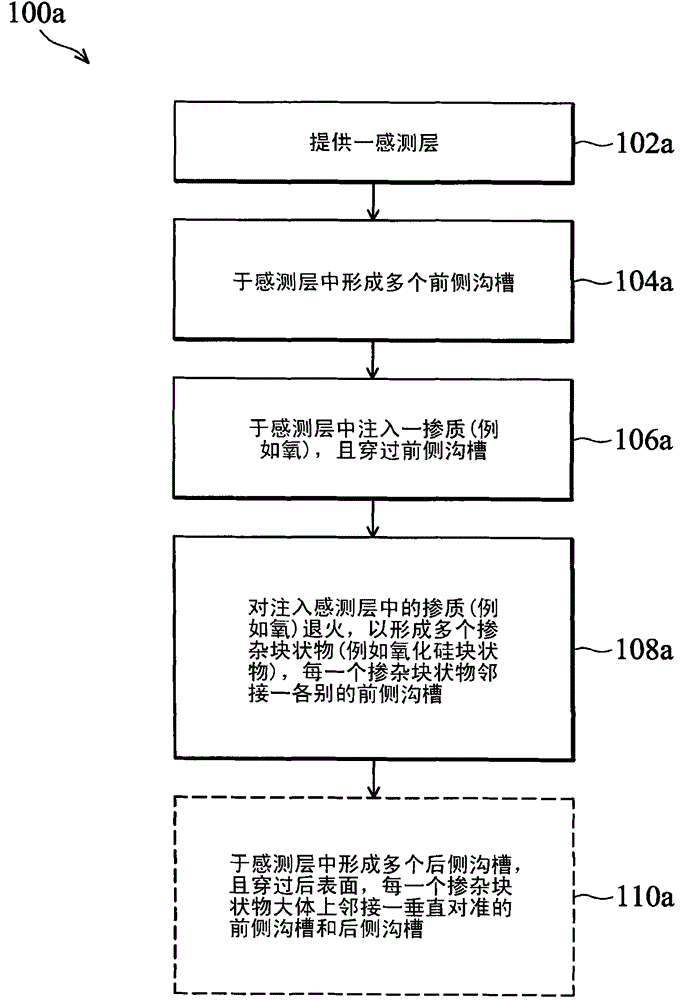
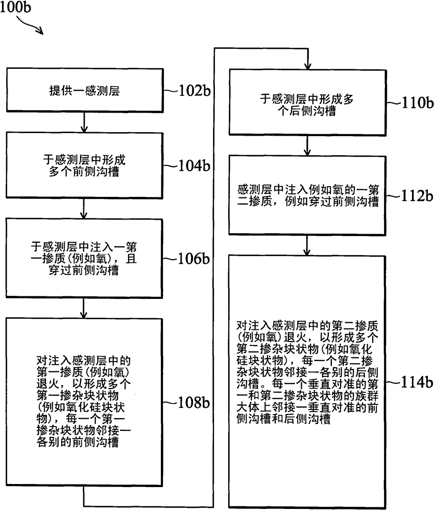
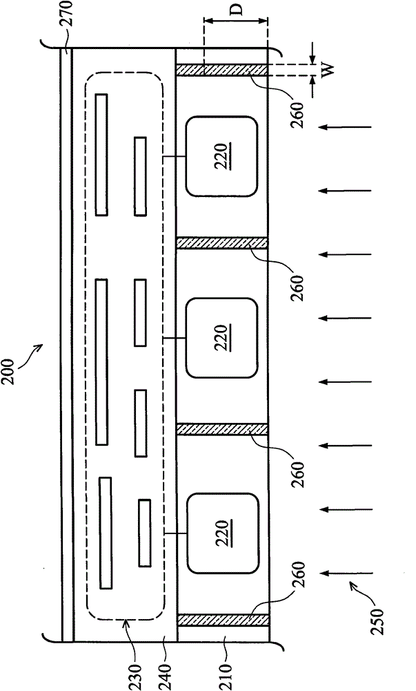
[0038] Please refer to the attached picture, Figure 1A with Figure 1B It is a flow chart of a method for manufacturing a semiconductor device including an isolation structure according to different embodiments of the present invention. Figure 2A with Figure 2B A schematic partial cross-sectional view and a plan view of a semiconductor device including a sensor isol...
PUM
 Abstract
Description
Claims
Application Information