Novel OLED display architecture

A technology of organic light-emitting devices and light-emitting materials, which is applied in semiconductor devices, electric solid-state devices, electrical components, etc., and can solve problems such as negative work function

Active Publication Date: 2011-10-19
UNIVERSAL DISPLAY
View PDF24 Cites 24 Cited by
  • Summary
  • Abstract
  • Description
  • Claims
  • Application Information

AI Technical Summary

Problems solved by technology

Since work functions are usually measured as negative numbers relative to the vacuum level, this means that "higher" work functions are more negative

Method used


Image

  • Novel OLED display architecture
  • Novel OLED display architecture
  • Novel OLED display architecture

Examples


Embodiment Construction

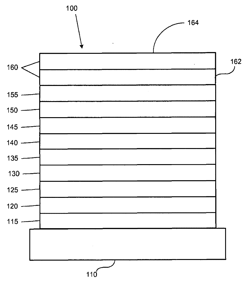
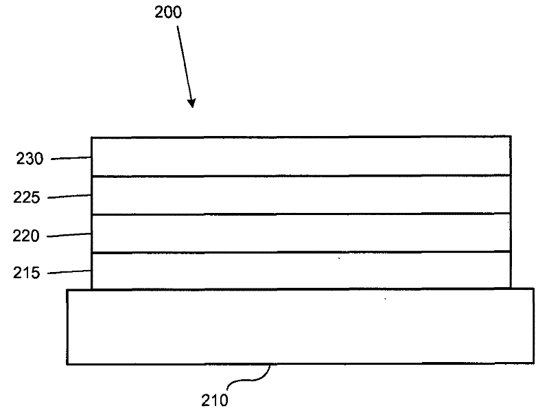
[0029] Typically, an OLED comprises at least one organic layer disposed between and electrically connected to an anode and a cathode. When a current is applied, the anode injects holes into the one or more organic layers and the cathode injects electrons into the one or more organic layers. Each of the injected holes and electrons migrates toward the oppositely charged electrode. When an electron and a hole localize on the same molecule, an "exciton" is formed, which is a localized electron-hole pair with an excited energy state. Light is emitted when the excitons relax through a photoemission mechanism. In some cases, the excitons can be localized to excited excimers or exciplexes. Non-radiative mechanisms also occur, such as thermal relaxation, but are generally considered unnecessary.

[0030] Initial OLEDs used light-emitting molecules that emitted light ("fluorescence") from their singlet states, as disclosed in US Patent No. 4,769,292, which is incorporated herein by ...


PUM


Abstract

A device that may be used as a multi-color pixel is provided. The device has a first organic light emitting device, a second organic light emitting device, a third organic light emitting device, and a fourth organic light emitting device. The device may be a pixel of a display having four sub-pixels. The first device may emit red light, the second device may emit green light, the third device may emit light blue light and the fourth device may emit deep blue light.

Description

[0001] This application claims priority and benefit under 35 U.S.C. § 119(e) to U.S. Provisional Application No. 61 / 101,757, filed October 1, 2008, the entire disclosure of which is incorporated herein by reference. [0002] This invention was made by, is responsible for, and / or is related to one or more of the following parties to a joint university collaborative research agreement: Directors of the University of Michigan, Princeton University, University of Southern California, and Universal Display Corporation. This agreement was in effect on and before the date the invention was made, which was made as a result of activities undertaken within the scope of this agreement. technical field [0003] The present invention relates to organic light emitting devices, and more particularly to the use of light blue and dark blue organic light emitting devices to exhibit color. Background technique [0004] Optoelectronic devices utilizing organic materials are becoming increasingl...

Claims


Application Information

Patent Timeline
Patent Type & Authority Applications(China)
IPC IPC(8): H01L27/32
CPCH10K59/351H10K59/352H10K50/11H10K2101/10C09K2211/185
Inventor M·哈克J·J·布朗M·S·韦弗B·德安德雷德
Owner UNIVERSAL DISPLAY
Why Eureka
Try Eureka