Check patentability & draft patents in minutes with Patsnap Eureka AI!

Encapsulation structure for light-emitting diode and manufacturing method thereof

A technology of light-emitting diodes and packaging structures, which is applied in the direction of electrical components, electric solid devices, circuits, etc., can solve the problems of inability to obtain phosphor layers, uneven light mixing of light emitted from the packaging structure of light-emitting diodes, etc., and improve the uniformity of light mixing Effect

Inactive Publication Date: 2014-07-02
ZHANJING TECH SHENZHEN +1
View PDF5 Cites 0 Cited by
  • Summary
  • Abstract
  • Description
  • Claims
  • Application Information

AI Technical Summary

Problems solved by technology

However, since a right angle is formed between the bottom wall and the side wall of the groove of the package carrier 2, the phosphor layer at the corner will have a relatively large thickness, and it is still impossible to obtain a phosphor layer with the same thickness, thereby causing the light-emitting diode The light emitted by the package structure will still be mixed and uneven

Method used


Image

  • Encapsulation structure for light-emitting diode and manufacturing method thereof
  • Encapsulation structure for light-emitting diode and manufacturing method thereof
  • Encapsulation structure for light-emitting diode and manufacturing method thereof

Examples


Embodiment Construction

[0032] The present invention will be further described in detail below in conjunction with the accompanying drawings.

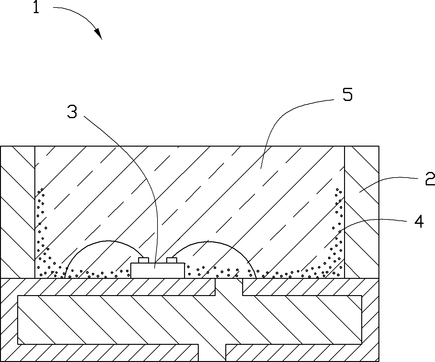
[0033] see figure 2 A light emitting diode package structure 10 provided in the first embodiment of the present invention includes a package carrier 11 , two lead frames 12 , a light emitting diode chip 13 , a first fluorescent layer 14 and a transparent colloid 15 .

[0034] The package carrier 11 includes a first surface 111 and a second surface 112 opposite to each other. An accommodating groove 113 is formed on the first surface 111 . The accommodating groove 113 is surrounded by a bottom wall 114 and a side wall 115 . The side wall 115 includes an arc-shaped concave surface 115 a, the arc-shaped concave surface 115 a is located at an end of the side wall 115 close to the bottom wall 114 , and is connected to the bottom wall 114 . Preferably, the bottom wall 114 is tangent to the arc concave surface 115a. The package carrier 11 can be made of high th...


PUM


Abstract

The invention relates to a method for manufacturing an encapsulation structure for a light-emitting diode, which comprises the following steps of: providing an encapsulation carrier and two lead frames, wherein the encapsulation carrier comprises a first surface, an accommodating groove is formed on the first surface, the accommodating groove is enclosed by a bottom wall and a side wall, the side wall comprises an arc-shaped concave surface, and the arc-shaped concave surface is connected with the bottom wall; adhering a light-emitting diode chip to the bottom wall of the accommodating groove, so that the light-emitting diode chip is electrically connected with the two lead frames; injecting transparent colloid mixed with fluorescent powder into the accommodating groove; precipitating the fluorescent powder in the transparent colloid on the surface of the light-emitting diode chip and on the bottom wall and the side wall of the accommodating groove by utilizing the centrifugal technology before the transparent colloid is cured to obtain a first fluorescent layer, wherein the thickness of the first fluorescent layer is approximately the same; and curing the transparent colloid. The invention also relates to the encapsulation structure for the light-emitting diode.

Description

technical field [0001] The invention relates to a semiconductor package structure, in particular to a light emitting diode package structure and a manufacturing method thereof. Background technique [0002] A general light emitting diode (Light Emitting Diode, LED) packaging structure is to mix phosphor powder in a transparent colloid and cover the light emitting diode chip to form white light or mixed light of multiple wavelengths. However, the light beams emitted from the light emitting diode chip in different directions pass through the transparent colloid at different distances, resulting in uneven mixing of light emitted from the light emitting diode packaging structure. For example, for a white light emitting diode package structure using blue light emitting diode chips and yellow phosphor, the central area of ​​the emitted light tends to be blue, while the peripheral area is yellowish. [0003] see figure 1 In order to solve the above problems, a light emitting diod...

Claims


Application Information

Patent Timeline
Patent Type & Authority Patents(China)
IPC IPC(8): H01L33/48H01L33/44
CPCH01L2224/48091H01L2224/48247H01L2224/8592H01L2924/181
Inventor 黄志强
Owner ZHANJING TECH SHENZHEN
Features
  • R&D
  • Intellectual Property
  • Life Sciences
  • Materials
  • Tech Scout
  • Unparalleled Data Quality
  • Higher Quality Content
  • 60% Fewer Hallucinations
Learn More