Testing structure and testing method for hot carrier effect of MOS (Metal Oxide Semiconductor) device

A technology of MOS device and test structure, applied in the field of test structure of MOS device hot carrier effect, can solve problems such as low test efficiency, and achieve the effects of improving test efficiency, improving test time, and saving stress loading time

Active Publication Date: 2011-11-23
SHANGHAI INTEGRATED CIRCUIT RES & DEV CENT
View PDF6 Cites 12 Cited by
  • Summary
  • Abstract
  • Description
  • Claims
  • Application Information

AI Technical Summary

Problems solved by technology

[0004] In summary, in the prior art, the test structure of the hot carrier effect of MOS devices has low test efficiency

Method used


Image

  • Testing structure and testing method for hot carrier effect of MOS (Metal Oxide Semiconductor) device
  • Testing structure and testing method for hot carrier effect of MOS (Metal Oxide Semiconductor) device
  • Testing structure and testing method for hot carrier effect of MOS (Metal Oxide Semiconductor) device

Examples


Embodiment 1

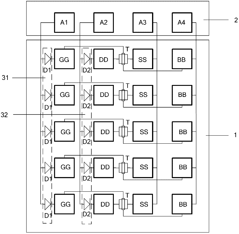
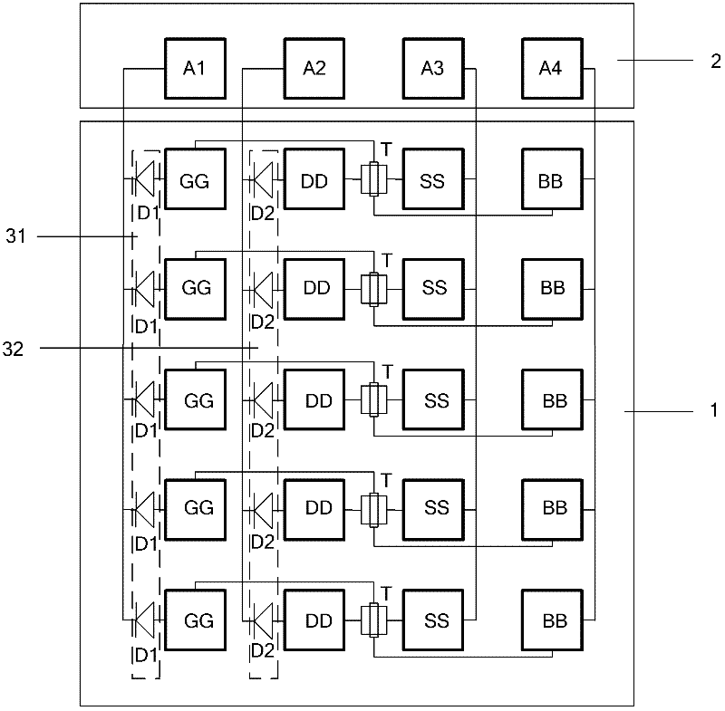
[0026] like figure 1 As shown, the test structure of the hot carrier effect of the MOS device of the present invention includes at least two groups of test structure units 1 of the array, and each group of test structure units 1 includes a gate terminal, a drain terminal, The source terminal, the gate pad GG electrically connected to the substrate, the drain pad DD, the source pad SS, and the substrate pad BB; the gate pad GG of each group of test structural units 1 passes through the first two The pole transistor D1 is reversely connected to the first pad A1, and the drain pad DD of each group of test structure units 1 is reversely connected to the second pad A2 through the second diode D2, and each group of test structure The source pad SS and the substrate pad BB of the cell 1 are connected to the third pad A3 and the fourth pad A4 respectively.

[0027] Wherein, the gate pad GG of each group of test structure units 1 is reversely connected to the first pad A1 through the ...

Embodiment 2

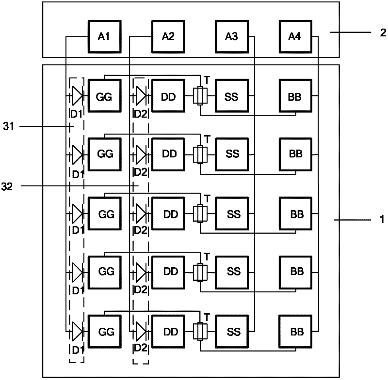
[0032] like figure 2 As shown, this embodiment 2 is improved on the basis of embodiment 1, and the difference is: the first diode connecting the gate pad GG of each group of test structure units 1 to the first pad A1 in reverse The tube D1 is changed to forward connection, and the second diode D2 reversely connected between the drain pad DD and the second pad A2 of each group of test structure units 1 is changed to forward connection. Wherein, the MOS device T is a P-type MOS device.

[0033] In Embodiment 2, after the gate pad GG is positively connected to the first pad A1 through the first diode D1, the voltage applied to the gate pad GG is a low level, and the drain pad DD is connected to the first pad A1 through the second diode D1. After the electrode transistor D2 is positively connected to the second pad A2, the voltage applied to the drain pad DD is low level. Therefore, this embodiment 2 is applicable to the hot carrier effect parameter test of the N-type MOS transi...


PUM


Abstract

The invention discloses a testing structure for a hot carrier effect of an MOS (Metal Oxide Semiconductor) device. The structure comprises at least two groups of arrayed test structure units (1), wherein a grid bonding pad (GG) of each group of the test structure unit (1) is connected with a first bonding pad (A1) through a first diode (D1); a drain bonding pad (DD) is connected with a second bonding pad (A2) through a second diode (D2); and a source bonding pad (SS) and a substrate bonding pad (BB) are connected with a third bonding pad (A3) and a fourth bonding pad (A4) respectively. The invention also discloses a method for testing the hot carrier effect by applying the parallel testing structure, and the method comprises the following steps: S1, testing a single device; S2, testing stress loading; S3, repeating tests of the step S1 and the step S2 alternately, and comparing electrical performance parameters of multiple measurements. By adopting the method, the testing efficiency of the hot carrier of the MOS device can be improved.

Description

technical field [0001] The invention relates to the field of semiconductor testing, in particular to a testing structure and testing method suitable for the hot carrier effect of MOS devices in wafers. Background technique [0002] When the semiconductor manufacturing process enters the deep submicron era, the reliability of semiconductor devices directly affects the performance and service life of the manufactured integrated circuit chips. Since hot carrier injection (HCI) is an important factor that has always affected the performance of MOS devices, it directly causes the degradation of the performance of MOS devices, so hot carrier injection has become an important indicator of reliability testing of MOS devices, that is, hot load Flow effect test. Hot carrier effect test, including stress loading stage test and single device stage test. The hot carrier injection of MOS devices is in accordance with the JEDEC standard. The stress loading stage test refers to applying a...

Claims


Application Information

Patent Timeline
IPC IPC(8): G01R31/26
Inventor 唐逸张悦强
Owner SHANGHAI INTEGRATED CIRCUIT RES & DEV CENT
Why Eureka
Try Eureka