backside illuminated cmos image sensor

An image sensor and backlighting technology, which is applied in the field of image sensors, can solve the problems of CMOS image sensor fading and affecting imaging quality, and achieve the effect of improving display fading, improving imaging quality, and reducing crosstalk of electrical signals

Inactive Publication Date: 2011-12-07
GALAXYCORE SHANGHAI
View PDF7 Cites 34 Cited by
  • Summary
  • Abstract
  • Description
  • Claims
  • Application Information

AI Technical Summary

Problems solved by technology

[0004] In practice, it is found that the above-mentioned back-illuminated CMOS image sensor has the problem of display fading, which affects the image quality

Method used


Image

  • backside illuminated cmos image sensor
  • backside illuminated cmos image sensor
  • backside illuminated cmos image sensor

Examples


Embodiment Construction

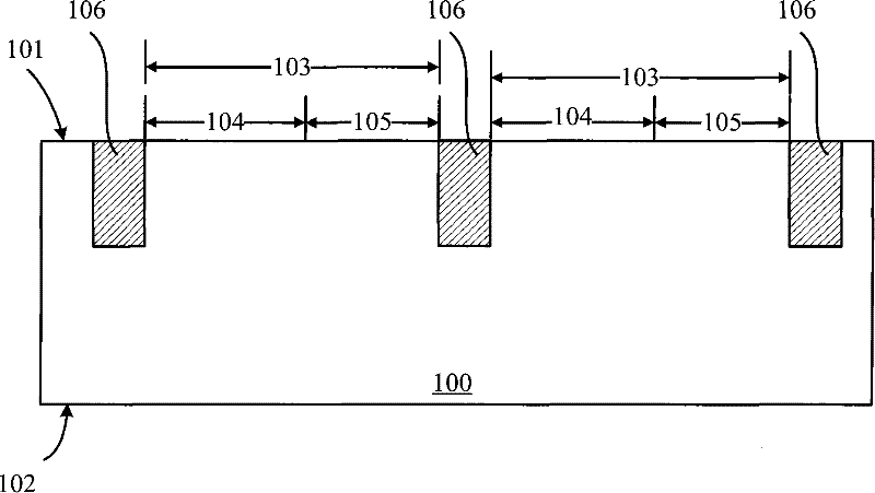
[0039] Existing backside illuminated (Backside illuminated) CMOS image sensors have the problem of display fading. The inventors found that the cause of fading is the crosstalk between adjacent pixels. One of the reasons for the crosstalk is that the existing shallow trench isolation structure cannot effectively isolate the diffusion of photo-generated carriers between adjacent pixel units. Since the incident light of the back-illuminated CMOS image sensor enters the pixel unit area of ​​the semiconductor substrate through the microlens and the optical filter, in the prior art, in order to improve the effective photosensitive area of ​​the photodiode in the pixel unit area, the depth of the photodiode is usually relatively small. Large, its depth can reach more than 10,000 angstroms, while the depth of existing shallow trench isolation structures is usually in the range of 2,000 to 5,000 angstroms. During the photoelectric conversion, the photo-generated carriers generated by...


PUM


Abstract

The present invention provides a backside illuminated CMOS image sensor, comprising: a semiconductor substrate having a first surface and a second surface opposite thereto; the semiconductor substrate includes at least one pixel unit region; an isolation structure located at Between adjacent pixel unit regions; wherein, the isolation structure is a deep trench isolation structure, and the deep trench isolation structure penetrates the first surface and the second surface of the semiconductor substrate. The invention reduces the crosstalk of electrical signals between adjacent pixel unit areas, improves the display fading of CMOS image sensors, and improves the imaging quality.

Description

technical field [0001] The present invention relates to image sensors, in particular to backside illuminated CMOS image sensors. Background technique [0002] The image sensor is an important part of the digital camera. According to different components, it is divided into a charge coupled (CCD, Charge Coupled Device) image sensor and a metal oxide semiconductor (CMOS, Complementary Metal-Oxide Semiconductor) image sensor. Among them, due to the high integration of the CMOS image sensor, it is easy to be compatible with the standard CMOS manufacturing process, and the power consumption is low. With the improvement of the CMOS manufacturing process, the CMOS image sensor has become the mainstream technology of the current image sensor. [0003] An existing CMOS image sensor is disclosed in Chinese patent application No. 200710148796.5. Existing CMOS image sensors include a semiconductor substrate, and the semiconductor substrate usually includes several pixel unit regions ar...

Claims


Application Information

Patent Timeline
Patent Type & Authority Applications(China)
IPC IPC(8): H01L27/146
Inventor 霍介光
Owner GALAXYCORE SHANGHAI
Why Eureka
Try Eureka