

Power device with side stage protecting source and gate and manufacture method thereof
A power device and gate-source technology, applied in the field of microelectronics, can solve the problems of poor reliability, poor economy and practicability, and high product cost of VDMOS power devices, and achieve convenient manufacturing, strong economy and practicability, The effect of simple structure
- Summary
- Abstract
- Description
- Claims
- Application Information
AI Technical Summary
Problems solved by technology
Method used
Image

Examples
Embodiment 1
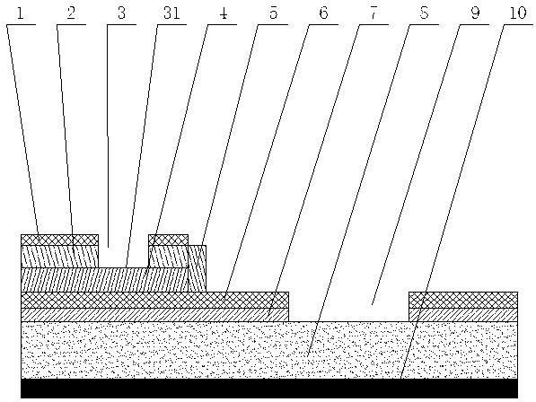
[0024] figure 1 is a schematic diagram of the internal structure of an embodiment of the present invention, figure 2 It is a process flow diagram of the present invention. Depend on figure 1 combine figure 2 It can be seen that the gate-source side platform protects the power device, which mainly includes a metal bottom layer 10 , a silicon wafer 8 , a thermally oxidized gate oxide layer 7 , a polysilicon layer 4 , a silicon dioxide layer 2 , and a thermally oxidized side platform 5 .
[0025] The silicon wafer 8 is used as a substrate layer to be thermally oxidized to grow a gate oxide layer 7 and a polysilicon layer 4, and a first silicon nitride layer 6 is grown under the polysilicon layer 4 as a protective layer under the polysilicon layer 4, and the polysilicon layer 4 acts as a gate conductive layer. Layer 31.
[0026] The silicon dioxide layer 2, the second silicon nitride layer 1 and the polysilicon layer 4 form a ring-shaped gate area, and the upper surface of t...
Embodiment 2
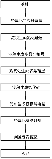
[0040] (1) Firstly, a layer of gate oxide layer is formed by thermal oxidation on the silicon wafer that has completed the conductive structure and terminal structure. The thermal oxidation temperature is 1000°, and the thickness of the gate oxide layer is 450 angstroms;
[0041] (2) On the gate oxide layer, a first silicon nitride layer is grown by deposition method as the lower protection layer of the polysilicon layer, and the thickness of the first silicon nitride layer is 650 angstroms;
[0042] (3) A polysilicon layer is grown as a gate electrode, and the thickness of the polysilicon layer is 10000 angstroms;
[0043] (4) The upper surface of the grown polysilicon layer is thermally oxidized to form a silicon dioxide layer, and the thickness of the silicon dioxide layer 2 is 5000 angstroms;
[0044] (5) A second silicon nitride layer is grown on the silicon dioxide layer as the upper protective layer of the polysilicon layer, and the thickness of the second silicon nitri...
Embodiment 3
[0050] (1) First, a gate oxide layer is formed by thermal oxidation on the silicon wafer that has completed the conductive structure and terminal structure. The thermal oxidation temperature is 1100°, and the thickness of the gate oxide layer is 600 angstroms;
[0051] (2) On the gate oxide layer, a first silicon nitride layer is grown by deposition method as the lower protection layer of the polysilicon layer, and the thickness of the first silicon nitride layer is 700 angstroms;
[0052] (3) A polysilicon layer is grown as a gate electrode, and the thickness of the polysilicon layer is 9500 angstroms;
[0053] (4) The upper surface of the grown polysilicon layer is thermally oxidized to form a silicon dioxide layer, and the thickness of the silicon dioxide layer 2 is 5500 angstroms;
[0054] (5) A second silicon nitride layer is grown on the silicon dioxide layer as the upper protective layer of the polysilicon layer, and the thickness of the second silicon nitride layer is 90...
PUM
 Abstract
Description
Claims
Application Information