Semiconductor light emitting diode and manufacturing method thereof

A technology of light-emitting diodes and semiconductors, applied in semiconductor devices, electrical components, circuits, etc., can solve the problems of reducing wavelength yield, wafer concave curvature, and reducing uniformity of light emission, so as to prevent growth defects, improve efficiency, and improve luminous efficiency Effect

Inactive Publication Date: 2011-12-14
LG DISPLAY CO LTD
View PDF4 Cites 2 Cited by
  • Summary
  • Abstract
  • Description
  • Claims
  • Application Information

AI Technical Summary

Problems solved by technology

[0024] Second, when the n-type GaN layer is grown to form the GaN epitaxial layer of the LED, the wafer may experience concave curvature
In this case, the emission uniformity of the active layer will be reduced, and the wavelength yield will be reduced

Method used


Image

  • Semiconductor light emitting diode and manufacturing method thereof
  • Semiconductor light emitting diode and manufacturing method thereof
  • Semiconductor light emitting diode and manufacturing method thereof

Examples


Embodiment Construction

[0044] The present invention will be described in detail below with reference to the accompanying drawings.

[0045] For the convenience of brief description with reference to the drawings, the same or equivalent components are given the same reference numerals, and their description will not be repeated.

[0046] Hereinafter, a semiconductor light emitting diode (LED) according to a preferred embodiment of the present invention is described in more detail with reference to the accompanying drawings.

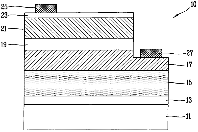
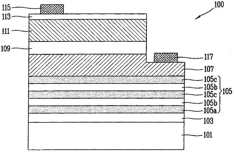
[0047] image 3 is a sectional view showing the structure of a semiconductor light emitting diode according to the present invention.

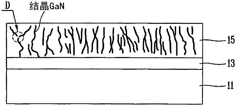
[0048] Such as image 3As shown, the semiconductor LED 100 of the present invention includes: a sapphire substrate 101; a buffer layer 103 formed on the sapphire substrate 101; a crystalline first semiconductor layer 105a based on undoped GaN, formed on the first semiconductor layer 105a An epitaxial layer 105 of one or more laminated structu...


PUM


Abstract

The invention discloses a semiconductor light emitting diode and a manufacturing method thereof. The method includes: forming a crystalline nitride semiconductor layer on a substrate; forming an amorphous layer and a crystalline nitride semiconductor layer on the nitride semiconductor layer; forming an n-type nitride semiconductor layer on the crystalline nitride semiconductor layer; forming an active layer on the compound semiconductor layer; and forming a p-type nitride semiconductor layer on the active layer.

Description

technical field [0001] The present invention relates to light emitting diodes, and more particularly to semiconductor light emitting diodes (LEDs) with improved epitaxial layers and methods of making the same. Background technique [0002] In general, a light emitting diode (LED) is a semiconductor device that converts received electrical energy into infrared light, ultraviolet light, and visible light using properties of compound semiconductors, such as recombination between electrons and holes. [0003] Such LEDs are generally used in home appliances, remote controllers, electronic display boards, display devices, various automatic devices, optical communications, and are mainly classified into infrared light emitting diodes (IREDs) and visible light emitting diodes (VLEDs). [0004] The frequency (or wavelength) of light emitted by an LED is a function of the bandgap of the material used in the semiconductor device. In the case of the use of narrow bandgap semiconductor ...

Claims


Application Information

Patent Timeline
Patent Type & Authority Applications(China)
IPC IPC(8): H01L33/02H01L33/32H01L33/12H01L33/42H01L33/00
CPCH01L33/32H01L33/16H01L33/12
Inventor 姜镐在郑多运金钟彬黃亨善朴清勋
Owner LG DISPLAY CO LTD
Why Eureka
Try Eureka