Single crystal diamond substrate structure and splicing processing method thereof

A single crystal diamond and substrate structure technology, applied in the direction of single crystal growth, single crystal growth, chemical instruments and methods, etc., can solve the problems of differences in grinding accuracy, inability to be closely arranged, cracking of joints, etc., to increase growth Surface, the effect of avoiding growth defects

Active Publication Date: 2021-04-30
XI AN JIAOTONG UNIV
View PDF4 Cites 0 Cited by
  • Summary
  • Abstract
  • Description
  • Claims
  • Application Information

AI Technical Summary

Problems solved by technology

[0004] However, this method is only the superposition of multiple small-sized diamond substrates. More importantly, there are differences in the internal structure and quality of multiple diamond substrates, which leads to problems such as cracking of the splicing seam and dislocation of crystal orientation.
In the process of processing, when diamond grinding technology is used to process the adjacent two sides, there is a risk of grinding cracking and chipping, the processing efficiency is low, and there are too many human experience problems, such as the difference in the grinding accuracy of two adjacent samples and the difference in the grinding parallelism cause it cannot be closely arranged, etc.

Method used


Image

  • Single crystal diamond substrate structure and splicing processing method thereof
  • Single crystal diamond substrate structure and splicing processing method thereof
  • Single crystal diamond substrate structure and splicing processing method thereof

Examples


Embodiment Construction

[0030] The present invention will be described in detail below in conjunction with the accompanying drawings and specific embodiments.

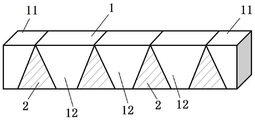
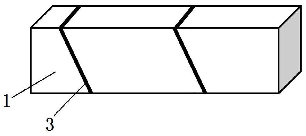
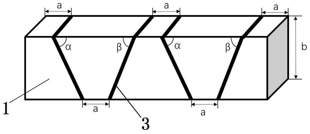
[0031] The invention discloses a splicing processing method of a single crystal diamond substrate structure, comprising the following steps: selecting a single crystal diamond substrate block; wherein, the single crystal diamond substrate block is in the shape of a cuboid, and its crystal orientation is ; The first growth plane of the single crystal diamond substrate block is the initial position, and the single crystal diamond substrate block is cut off; wherein, the section of the single crystal diamond substrate block is a plane, and the section extends from the first growth plane to the opposite side The second growth plane; take the axis parallel to the first growth plane as an axis, turn any block in the cutting block of the adjacent single crystal diamond substrate after cutting, so that the first growth face of a cutting block is adjac...


PUM

PropertyMeasurementUnit
sizeaaaaaaaaaa

Abstract

The invention discloses a single crystal diamond substrate structure and a splicing processing method thereof. The method comprises the steps: selecting a single crystal diamond substrate block; cutting off the single crystal diamond substrate block by taking the first growth surface of the single crystal diamond substrate block as an initial position, wherein the section of the single crystal diamond substrate block is a plane, and the section extends from the first growth surface to the second growth surface opposite to the first growth surface; turning over any one of the cut blocks of the adjacent single crystal diamond substrate by taking the axis parallel to the first growth surface as an axis, so that the first growth surface of one cut block and the second growth surface of the adjacent cut block are positioned on the same continuous plane; splicing the adjacent cut blocks after overturning, and taking a continuous plane as a growth surface; the same single crystal diamond substrate block is obliquely cut, and the cut blocks are turned over to form a new single crystal diamond substrate structure, so that the growth surface of the single crystal diamond substrate block can be effectively increased, and the growth defects of diamond can be avoided through the structure.

Description

technical field [0001] The invention belongs to the technical field of semiconductor device processing, and in particular relates to a single crystal diamond substrate structure and a splicing processing method thereof. Background technique [0002] Diamond has excellent characteristics such as ultra-wide bandgap (5.45eV), high breakdown field strength (20MV / cm), high carrier saturation drift velocity and carrier mobility, and its quality factor of microwave power devices is 4500 times higher than that of GaAs Silicon is 32,400 times higher, and it is expected to overcome the two major technical bottlenecks of "thermal effect" and "avalanche breakdown" of power electronic devices in radar T / R components at this stage. Therefore, it has shown obvious advantages and strong industrial potential as an ultra-wide and tight-band semiconductor material. At present, the size of single crystal diamond synthesized on the market is usually 5-10 mm, or even smaller. Large-sized single...

Claims


Application Information

Patent Timeline
Patent Type & Authority Applications(China)
IPC IPC(8): C30B33/06C30B23/02C30B25/18C30B29/04
CPCC30B33/06C30B23/025C30B25/18C30B29/04
Inventor 张晓凡王宏兴魏强
Owner XI AN JIAOTONG UNIV
Why Eureka
Try Eureka