Semiconductor device and manufacturing method thereof

A device manufacturing method and semiconductor technology, applied in the direction of semiconductor devices, electrical solid devices, electrical components, etc., can solve the problems of insufficient gate dielectric layer, device reliability degradation, device failure, etc., to avoid growth defects , the effect of improving reliability

Active Publication Date: 2021-07-13
YANGTZE MEMORY TECH CO LTD
View PDF0 Cites 0 Cited by
  • Summary
  • Abstract
  • Description
  • Claims
  • Application Information

AI Technical Summary

Problems solved by technology

However, in some step areas away from the core area ( Figure 1d middle left), due to the increase in substrate over-etching, the deposited and grown semiconductor layer is not enough to meet the above requirements, so that the gate dielectric layer is not enough to completely fill the boss 1ED during the subsequent process of removing layer 2A to form a gate stack The gap between the gate conductive layer and the second dielectric layer 2B may directly contact and electrically connect the boss 1ED, resulting in device failure
[0009] In addition, since the etchant penetrates the dielectric stack 2A / 2B to reach the substrate earlier in the step region, more etchant will laterally erode the dielectric stack before the core region is etched, which causes the step region There are a large number of hole defects on the side wall of channel hole 3HD, which will affect the quality of the film and reduce the reliability of the device in the subsequent epitaxy of the boss or vertical channel layer

Method used


Image

  • Semiconductor device and manufacturing method thereof
  • Semiconductor device and manufacturing method thereof
  • Semiconductor device and manufacturing method thereof

Examples


Embodiment Construction

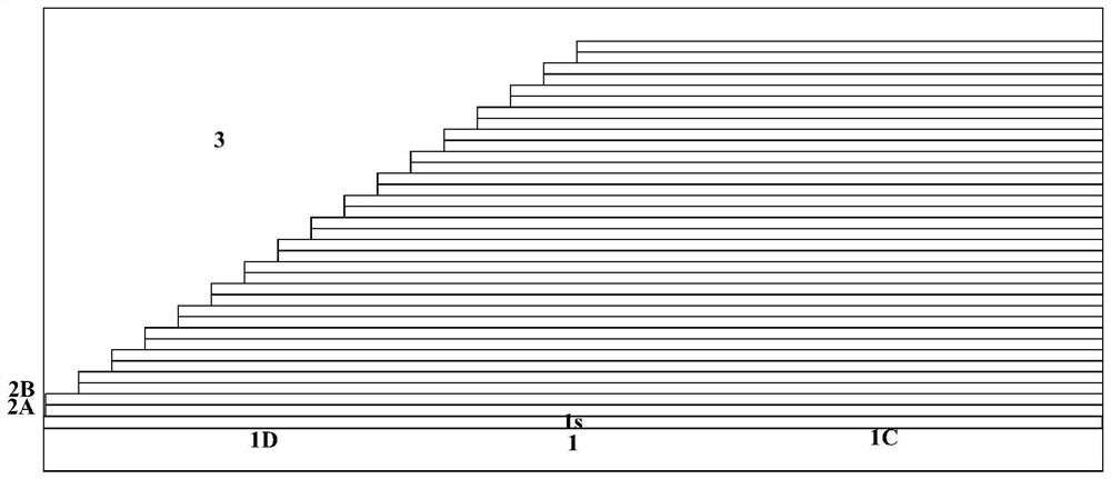
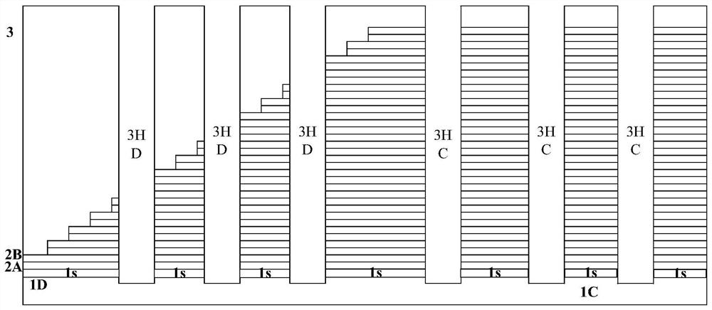
[0035] The features and technical effects of the technical solution of the present invention will be described in detail below with reference to the accompanying drawings and in conjunction with schematic embodiments, and a semiconductor device and a manufacturing method thereof that can effectively improve the reliability of a 3D NAND storage device are disclosed. It should be pointed out that similar reference numerals represent similar structures, and the terms "first", "second", "upper", "lower" and the like used in this application can be used to modify various device structures. These modifications do not imply a spatial, sequential or hierarchical relationship of the modified device structures unless specifically stated.

[0036] Such as Figure 2aAs shown, a substrate 10 is provided, and its material may include bulk silicon (bulk Si), bulk germanium (bulk Ge), silicon-on-insulator (SOI), germanium-on-insulator (GeOI) or other compound semiconductor substrates, such as...


PUM


Abstract

The invention discloses a semiconductor device, comprising: a substrate; a conductor / insulator stack, arranged on the substrate, composed of conductive layers and insulating layers alternately stacked along a first direction, including core regions arranged side by side along a second direction and the stepped area, the thickness of the core area along the first direction is constant, and the thickness of the stepped area along the first direction decreases gradually with the increase of the distance from the core area in the second direction; the first direction is perpendicular to the substrate The direction of the surface, the second direction is a direction parallel to the surface of the substrate; a plurality of storage channel regions vertically penetrate the core region of the conductor / insulator stack along the first direction; a plurality of dummy channel regions extend along the first direction The direction vertically runs through the step region of the conductor / insulator stack and contacts the substrate; a plurality of dummy channel regions are made of insulating material. The invention utilizes masks to respectively etch and fill the core area and the step area, avoids the epitaxial layer growth defect at the bottom of the step area, and improves the reliability of the device.

Description

technical field [0001] The invention relates to a semiconductor device and a manufacturing method thereof, in particular to a three-dimensional NAND memory unit transistor and a manufacturing method thereof. Background technique [0002] In order to improve the density of memory devices, the industry has made extensive efforts to develop methods of reducing the size of two-dimensionally arranged memory cells. As the size of memory cells in two-dimensional (2D) memory devices continues to shrink, signal collisions and interference can increase significantly, making it difficult to perform multi-level cell (MLC) operations. In order to overcome the limitations of 2D memory devices, the industry has developed memory devices with a three-dimensional (3D) structure to increase integration density by three-dimensionally arranging memory cells on a substrate. [0003] A cross-sectional view of a typical 3D NAND device structure during fabrication is shown in Figure 1a ~ Figure 1d...

Claims


Application Information

Patent Timeline
Patent Type & Authority Patents(China)
IPC IPC(8): H01L27/11551H01L27/11578
CPCH10B41/20H10B43/20
Inventor 隋翔宇陆智勇赵新梅王恩博霍宗亮王孝进
Owner YANGTZE MEMORY TECH CO LTD
Why Eureka
Try Eureka