A chip fault detection method and device
A fault detection and chip technology, applied in measuring devices, measuring electrical variables, measuring current/voltage, etc., can solve problems affecting the normal operation of electronic products or electronic equipment
- Summary
- Abstract
- Description
- Claims
- Application Information
AI Technical Summary
Problems solved by technology
Method used
Image
Examples
Embodiment 1
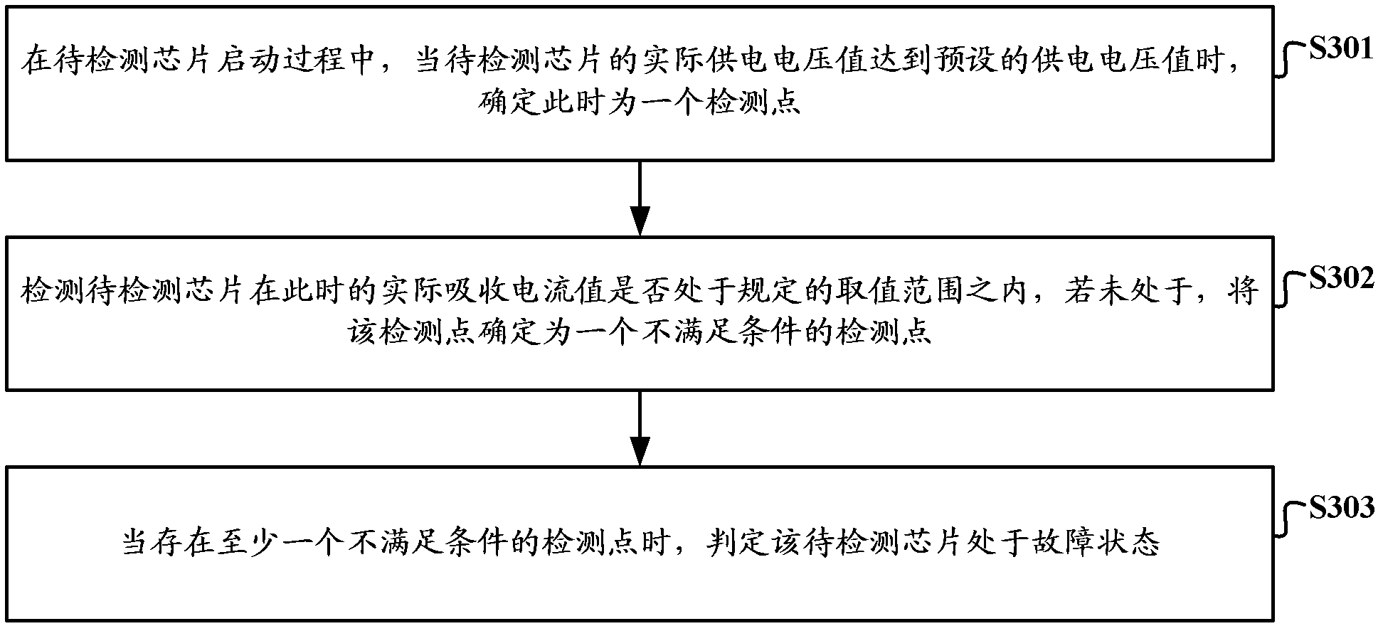
[0033] Such as image 3 As shown, it is a schematic diagram of the implementation flow of the chip fault detection method provided by the embodiment of the present invention, including the following steps:
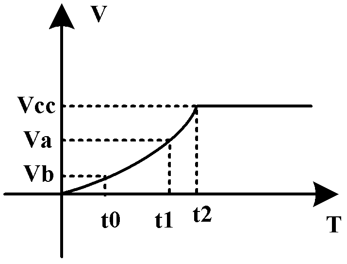
[0034] S301. During the start-up process of the chip to be detected, when the actual power supply voltage value of the chip to be detected reaches a preset power supply voltage value, determine that this is a detection point;
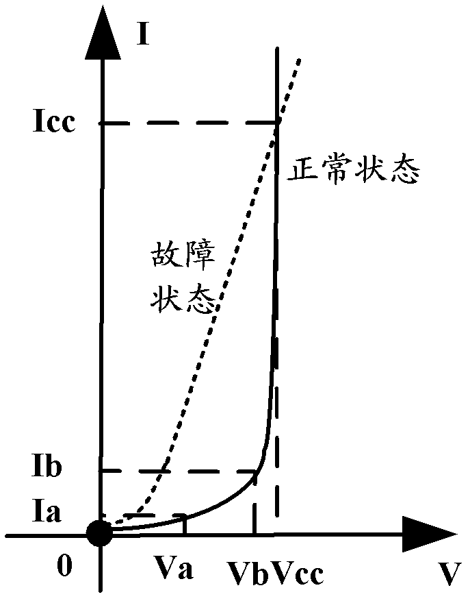
[0035] S302. Detect whether the actual absorbed current value of the chip to be detected at this time is within the specified value range, if not, determine the detection point as a detection point that does not meet the conditions;
[0036]S303. When there is at least one detection point that does not satisfy the condition, determine that the chip to be detected is in a failure state.
[0037] During specific implementation, in order to ensure the accuracy of chip fault detection, multiple detection points may be selected for detection during the ...
Embodiment 2
[0048] In the embodiment of the present invention, a chip fault detection device is described.
[0049] Such as Figure 5 As shown, the structural diagram of the chip fault detection device provided for the implementation of the present invention includes a current conversion unit 501, a determination unit 502 and at least one detection unit 503, and the detection units 503 are connected in parallel, wherein:
[0050] A current conversion unit 501, configured to convert the actual power supply voltage value of the chip to be detected into an output actual sink current value;
[0051] Each detection unit 503 is used to determine that this time is a detection point when the actual power supply voltage value of the chip to be detected reaches the preset power supply voltage value during the start-up process of the chip to be detected; and detect that the chip to be detected is at this time Whether the actual absorption current value of the test is within the specified value rang...
Embodiment 3
[0055] In the embodiment of the present invention, the specific structure of the detection unit 503 is described.
[0056] Such as Figure 6 Shown is a schematic structural diagram of the detection unit 503, including: a first comparator 5031, a second comparator 5032, a third comparator 5033, a first flip-flop 5034, a second flip-flop 5035 and a determination module 5036, wherein:
[0057] The negative input terminal of the first comparator 5031 is connected with the constant voltage source, and receives the corresponding supply voltage value at the determined detection point; the positive input terminal of the first comparator 5031 is connected with the supply voltage value of the chip to be detected, for Receive the actual power supply voltage value of the chip to be detected; the output terminal of the first comparator 5031 is connected with the CLK pins of the first flip-flop 5034 and the second flip-flop 5035 respectively, for when the actual power supply voltage value o...
PUM
 Abstract
Description
Claims
Application Information


