
Memory with bit line current injection

a technology of memory and current injection, applied in the field of memory implementation, can solve the problems of failure to read properly and lower manufacturing yield

Active Publication Date: 2013-09-05
APPLE INC
View PDF2 Cites 5 Cited by
  • Summary
  • Abstract
  • Description
  • Claims
  • Application Information

AI Technical Summary

Benefits of technology

The patent describes a memory circuit with a current injector that can control the current levels sent to a sense amplifier for amplifying data. The current injector can also sink current from the output of the sense amplifier. The circuit can store data and compare it with the original data to determine the strength of the data storage cell. The technical effect of this invention is to enhance the accuracy and reliability of memory circuits by ensuring consistent amplification of data and monitoring the strength of the data storage cell.

Problems solved by technology

Data from data storage cells that generate a smaller than average output signal due to the previously described variation may not be able to be read correctly, resulting in a misread.
Data storage cells that fail to read properly may contribute to lower manufacturing yield and necessitate additional redundant data storage cells to maintain manufacturing yield goals.

Method used


Image

  • Memory with bit line current injection
  • Memory with bit line current injection
  • Memory with bit line current injection

Examples


Embodiment Construction

[0023]During the manufacture of a semiconductor memory circuit, differences in lithography, implant levels, etc., may result in differences in electrical characteristics between data storage cells that are otherwise intended to be identical in characteristics and performance. In some cases, the variation of the electrical characteristics of a data storage cell may be sufficiently large that the data storage cell may not function (e.g., read or write) under normal operating conditions of the memory circuit, resulting in the data storage cell being identified as a failure and requiring replacement with a redundant data storage cell. Adding redundant data storage cells to the memory circuit to compensate for data storage cells with non-ideal electrical characteristics may result in additional chip area and power consumptions. The embodiments illustrated below may provide techniques to identify and compensate for data storage cells with non-ideal electrical characteristics.

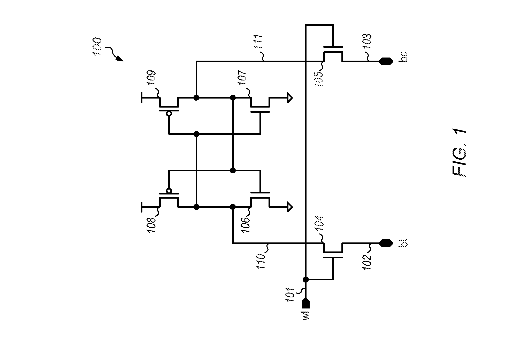
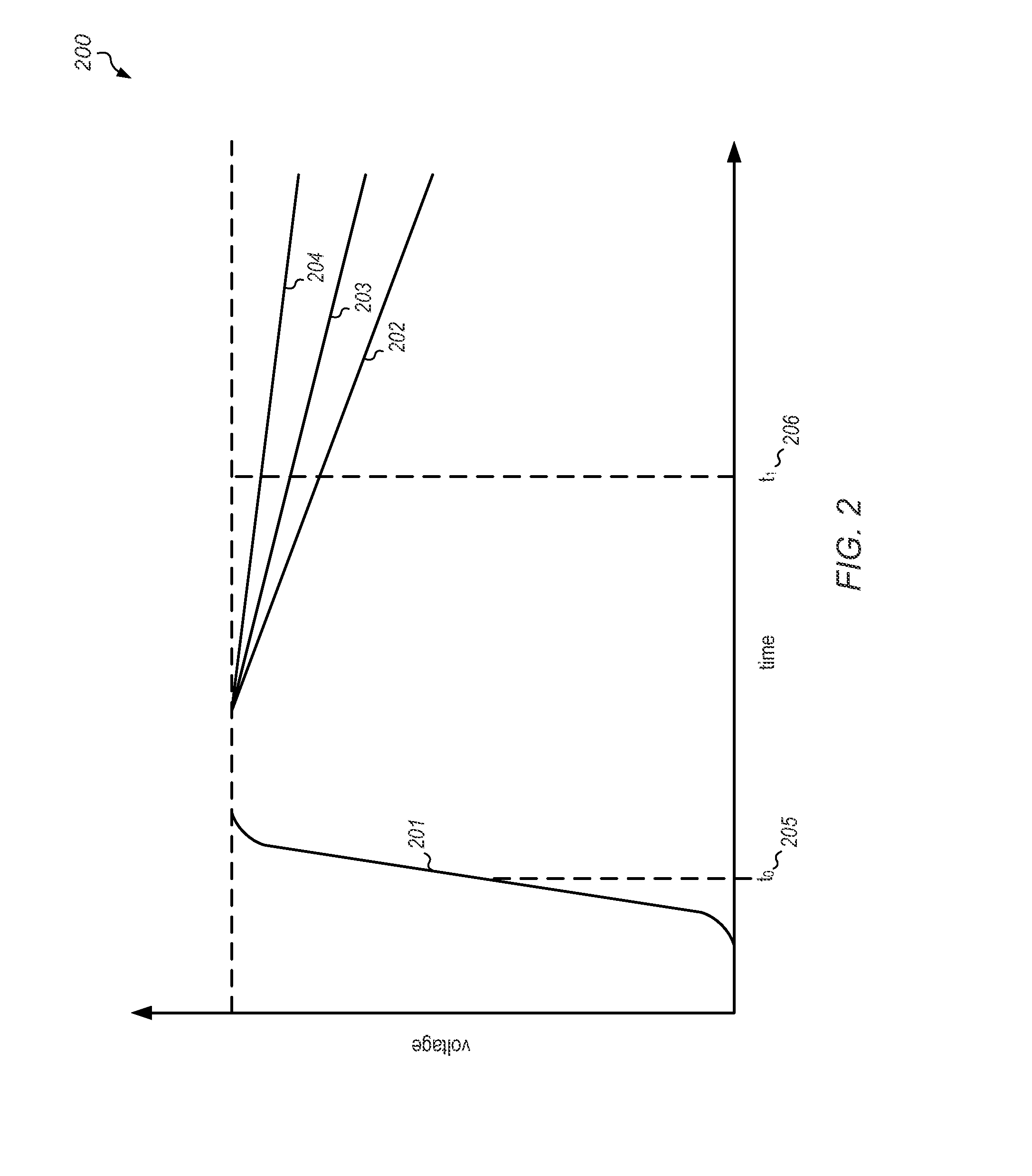
[0024]FIG. 1 ...


PUM


Abstract

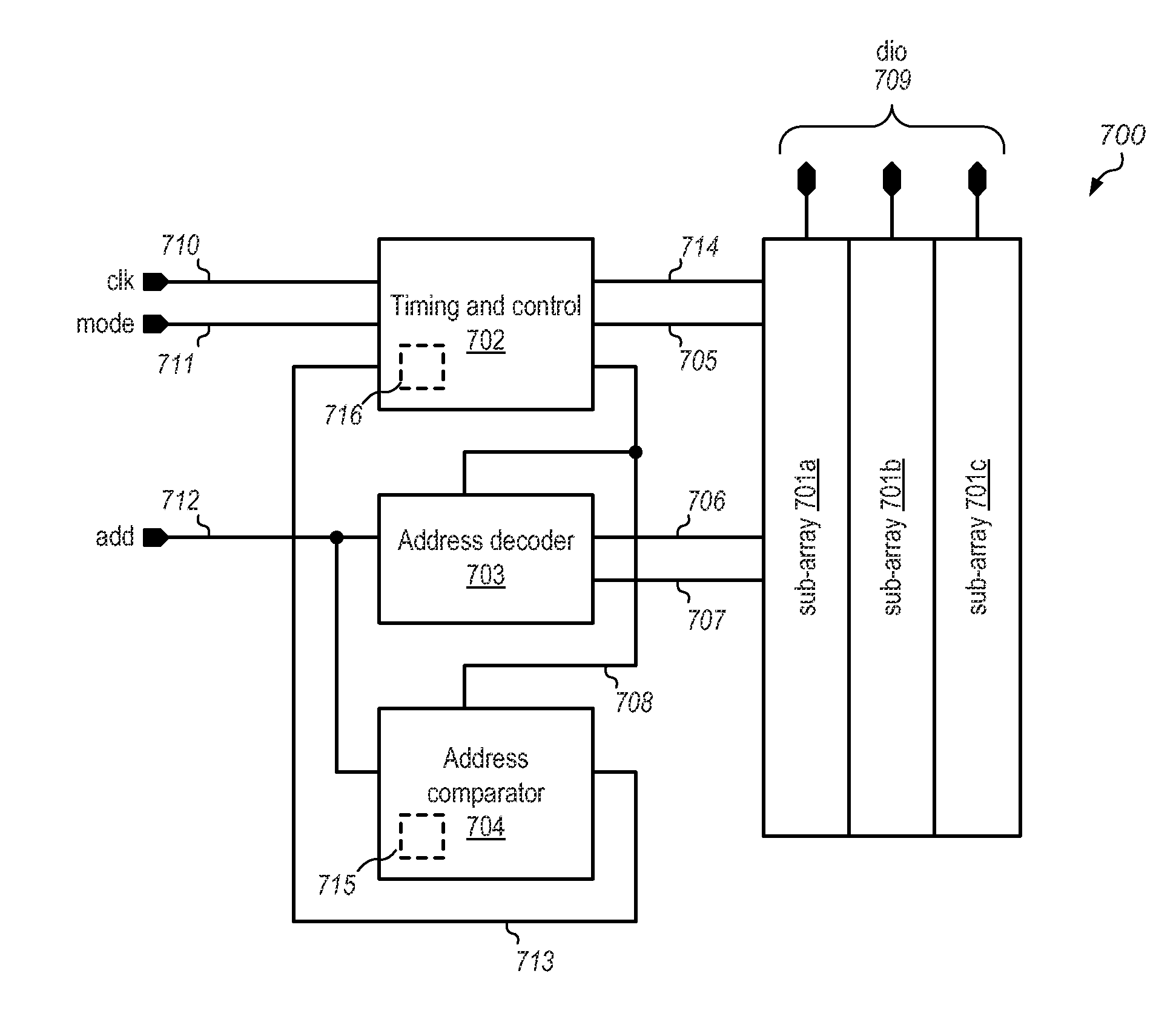
Embodiments of a memory are disclosed that may allow for the detection of weak data storage cells or may allow operation of data storage cells under conditions that may represent the effects of transistor ageing. The memory may include data storage cells, a column multiplexer, a sense amplifier, and a current injector. The current injector may be configured to generate multiple current levels and may be operable to controllably select one of the current levels to either source current to or sink current from the input of the sense amplifier.

Description

BACKGROUND[0001]1. Technical Field[0002]This invention is related to the field of memory implementation, and more particularly to techniques for data storage cell testing.[0003]2. Description of the Related Art[0004]Memories typically include a number of data storage cells composed of interconnected transistors fabricated on a semiconductor substrate. Such data storage cells may store a single data bit or multiple data bits and may be constructed according to a number of different circuit design styles. For example, the data storage cells may be implemented as a single transistor coupled to a capacitor to form a dynamic storage cell. Alternatively, cross-coupled inverters may be employed to form a static storage cell or a floating gate MOSFET may be used to create a non-volatile storage cell.[0005]During the semiconductor manufacturing process, variations in lithography, transistor dopant levels, etc., may result in different electrical characteristics between transistors that are i...

Claims


Application Information

Patent Timeline
IPC IPC(8): G11C29/00G11C7/06G11C7/10
CPCG11C7/06G11C11/41G11C2029/5002G11C29/50G11C2029/1204G11C29/12
Inventor SENINGEN, MICHAEL R.RUNAS, MICHAEL E.
Owner APPLE INC
Learn More