Quad flat no-lead package and manufacturing method thereof

A leadless packaging, square flat technology, applied in semiconductor/solid-state device manufacturing, electrical solid-state devices, semiconductor devices, etc., can solve problems such as chip electrode prolapse, thermal stress residue, etc., to reduce thermal stress, save costs, The effect of saving joint reinforcement structure

Inactive Publication Date: 2011-12-21
SHANGHAI KAIHONG ELECTRONICS CO LTD +2
View PDF5 Cites 3 Cited by
  • Summary
  • Abstract
  • Description
  • Claims
  • Application Information

AI Technical Summary

Problems solved by technology

[0004] attached figure 1 The disadvantage of the prior art shown is that the chip electrode is easy to come out of the plastic package, especially when the chip is working due to temperature changes and the deformation between the chip electrode and the plastic package due to the difference in thermal expansion coefficient occurs. , this phenomenon is particularly obvious, and due to the thermal expansion coefficient mismatch between the chip tray and the chip electrode and the plastic package, it will cause serious thermal stress residual problems

Method used


Image

  • Quad flat no-lead package and manufacturing method thereof
  • Quad flat no-lead package and manufacturing method thereof
  • Quad flat no-lead package and manufacturing method thereof

Examples


Embodiment Construction

[0014] A specific implementation of a quad flat no-lead package and its manufacturing method provided by the present invention will be described in detail below with reference to the accompanying drawings.

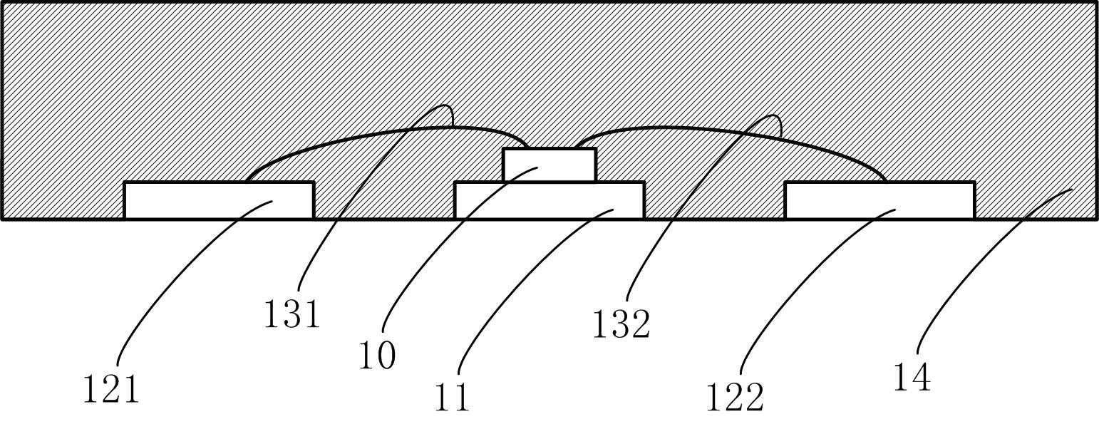
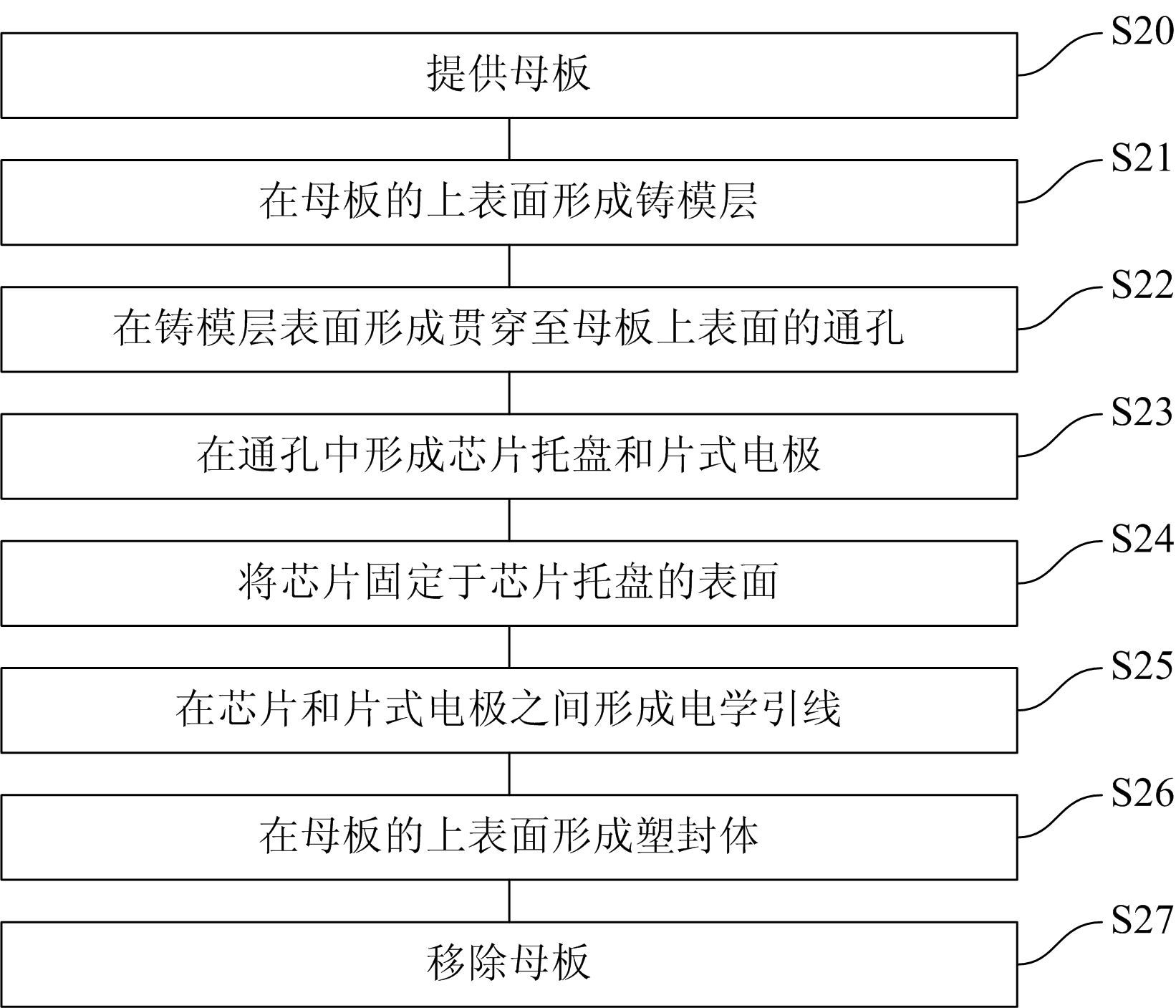
[0015] attached figure 2 Shown is a schematic diagram of the implementation steps of the specific embodiment of the method of the present invention, including the following steps: step S20, providing a motherboard; step S21, forming a mold layer on the upper surface of the motherboard; step S22, forming a through-to A through hole on the upper surface of the motherboard; step S23, forming a chip tray and a chip electrode in the through hole; step S24, fixing the chip on the surface of the chip tray; step S25, forming an electrical lead between the chip and the chip electrode; Step S26, forming a plastic package on the upper surface of the motherboard; step S27, removing the motherboard to expose the chip tray and chip electrodes embedded in the plastic package.

[0016] ...


PUM


Abstract

The invention provides a method for manufacturing a quad flat no-lead package, comprising the following steps: providing a motherboard; forming a mold layer on the upper surface of the motherboard; forming a through hole penetrating to the upper surface of the motherboard on the surface of the mold layer, The opening area of ​​the through hole close to the upper surface of the motherboard is smaller than the opening area of ​​the other side; the chip tray and the chip electrode are formed in the through hole; the chip is fixed on the surface of the chip tray; between the chip and the chip electrode forming electrical leads between them; forming a plastic package on the upper surface of the motherboard; removing the motherboard to expose the chip tray and chip electrodes embedded in the plastic package.

Description

technical field [0001] The invention relates to the field of packaging and testing of semiconductor devices, in particular to a quadrilateral flat leadless package and a manufacturing method thereof. Background technique [0002] In everyday life, consumers demand more and more reliability, size, and price from products such as personal phones, personal digital assistants, and music players. For example, consumers want their personal phones to be ultra-thin and reliable. This requires packaged devices to be smaller and have fewer defects. In addition, these small form factor requirements may also require electronic components that dissipate heat from the packaging structure. [0003] Quad flat no-lead package is a common packaging method in the prior art. The method is a standard packaging method using one lead frame and one die. attached figure 1 Shown is a schematic cross-sectional view of a typical QFN package structure in the prior art, including a chip 10 , a chip ...

Claims


Application Information

Patent Timeline
Patent Type & Authority Applications(China)
IPC IPC(8): H01L21/60H01L23/488
CPCH01L2924/18301H01L2224/48247H01L2224/48091H01L2924/00014
Inventor 高洪涛张元发张江元
Owner SHANGHAI KAIHONG ELECTRONICS CO LTD
Why Eureka
Try Eureka