Supercharge Your Innovation With Domain-Expert AI Agents!

Continuous high temperature chemical vapor deposition (HTCVD) method silicon carbide crystal growing device

A technology of crystal growth and silicon carbide, which is applied in crystal growth, single crystal growth, single crystal growth, etc., can solve the problems of low growth efficiency and unsatisfactory industrial scale development.

Active Publication Date: 2013-09-18
INST OF SEMICONDUCTORS - CHINESE ACAD OF SCI
View PDF4 Cites 0 Cited by
  • Summary
  • Abstract
  • Description
  • Claims
  • Application Information

AI Technical Summary

Problems solved by technology

The traditional silicon carbide crystal growth device usually only grows one crystal ingot (crystal rod) per furnace, and the general growth device is intermittent, that is, the raw material is heated and grown after being loaded into the furnace, and the temperature is lowered after the growth is completed, and it cannot be started until room temperature. The ingot is taken out of the furnace; relatively speaking, the growth efficiency is low, which cannot meet the huge demand of industrial scale development

Method used


Image

  • Continuous high temperature chemical vapor deposition (HTCVD) method silicon carbide crystal growing device
  • Continuous high temperature chemical vapor deposition (HTCVD) method silicon carbide crystal growing device
  • Continuous high temperature chemical vapor deposition (HTCVD) method silicon carbide crystal growing device

Examples


Embodiment Construction

[0023] Exemplary embodiments of the present invention will be described below with reference to the accompanying drawings. For the sake of clarity and brevity, actual embodiments are not limited to the technical features described in the specification. It should be understood, however, that in improving any one of the actual embodiments described, multiple embodiment-specific decisions must be made to achieve the improver's specific goals, for example, compliance with industry-related and business-related constraints, described Limits vary from embodiment to embodiment. Moreover, it should be understood that the effects of the aforementioned improvements, even if very complex and time-consuming, are still routine technical means for those skilled in the art who are aware of the benefits of the present invention.

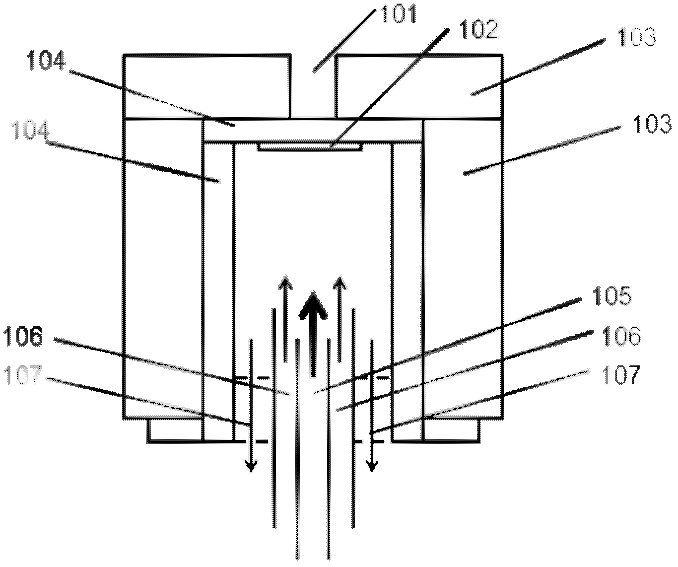
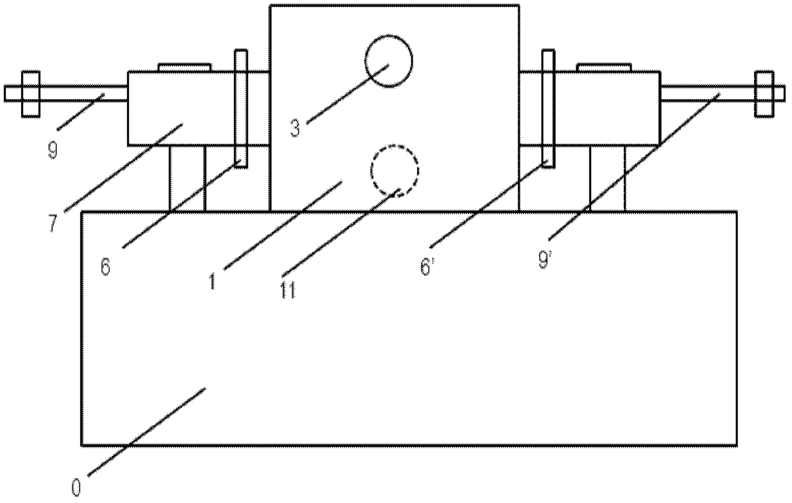
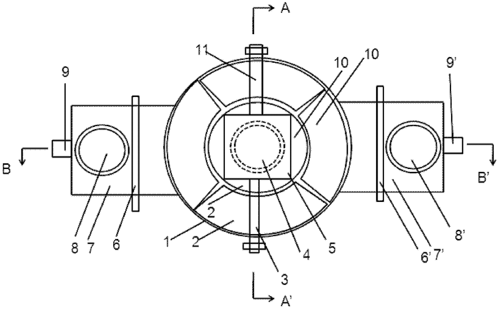
[0024] see Figure 2 to Figure 5 as shown in figure 2 , the continuous crystal growth device comprises: a main chamber 1, which is a cylindrical hollow body, use...


PUM


Abstract

The invention relates to a continuous high temperature chemical vapor deposition (HTCVD) method silicon carbide crystal growing device. The device comprises a main chamber, a moveable tray, a fixed tray, a first auxiliary chamber and a second auxiliary chamber, wherein the main chamber is a hollow cylinder and used for providing a vacuum environment for crystal growth; a tail gas pipeline radially passes through the main chamber; a source gas pipeline is communicated with the lower part of the tail pipeline; the moveable tray is positioned in the main chamber and above the source gas pipeline; the fixed tray is positioned in the main chamber and above the moveable tray; the first auxiliary chamber is used for providing a vacuum buffer environment and provides a sample to the main chamber under the environment; the first auxiliary chamber is positioned on one side of the main chamber and is communicated with the main chamber; a first gate is arranged between the main chamber and the first auxiliary chamber; a second auxiliary chamber is used for providing a vacuum buffer environment and taking out the sample from the main chamber under the environment; the second auxiliary chamber is arranged on the other side of the main chamber and is communicated with the main chamber; a second gate is arranged between the main chamber and the second auxiliary chamber; and the first auxiliary chamber and the second auxiliary chamber are isolated from the main chamber respectively through the first gate and the second gate.

Description

technical field [0001] The present invention relates to the field of semiconductor technology, in particular to a continuous high temperature chemical vapor deposition (High Temperature Chemical Vapor Deposition, HTCVD) silicon carbide crystal growth device or a halide chemical vapor deposition (Halogen Chemical Vapor Deposition, HCVD) silicon carbide crystal growing device. Background technique [0002] Silicon carbide (SiC) is the third-generation semiconductor material developed after the first-generation semiconductor materials silicon (Si), germanium (Ge) and the second-generation semiconductor material gallium arsenide (GaAs). Since SiC has the characteristics of three times the wide bandgap of Si, ten times the high critical breakdown electric field of Si, three times the high thermal conductivity of Si, and twice the high carrier saturation concentration of Si, it is widely used in military and aerospace applications. It has superior application value in high temper...

Claims


Application Information

Patent Timeline
Patent Type & Authority Patents(China)
IPC IPC(8): C30B29/36C30B25/00
Inventor 刘兴昉郑柳董林闫果果王雷赵万顺孙国胜曾一平李晋闽
Owner INST OF SEMICONDUCTORS - CHINESE ACAD OF SCI
Features
  • R&D
  • Intellectual Property
  • Life Sciences
  • Materials
  • Tech Scout
  • Unparalleled Data Quality
  • Higher Quality Content
  • 60% Fewer Hallucinations
Learn More