Check patentability & draft patents in minutes with Patsnap Eureka AI!

TFT array inspection method and TFT array inspection apparatus

An inspection method and array technology, applied in the direction of measuring devices, identification devices, electronic circuit testing, etc., to achieve the effect of improving the defect detection rate, eliminating the influence of pixel voltage, and prolonging the voltage holding time

Inactive Publication Date: 2012-01-04
SHIMADZU SEISAKUSHO CO LTD
View PDF7 Cites 5 Cited by
  • Summary
  • Abstract
  • Description
  • Claims
  • Application Information

AI Technical Summary

Problems solved by technology

[0009] In addition, in addition to the above-mentioned defects in each pixel, there is also a defect called an adjacent defect that occurs between adjacent pixels.

Method used


Image

  • TFT array inspection method and TFT array inspection apparatus
  • TFT array inspection method and TFT array inspection apparatus
  • TFT array inspection method and TFT array inspection apparatus

Examples


Embodiment Construction

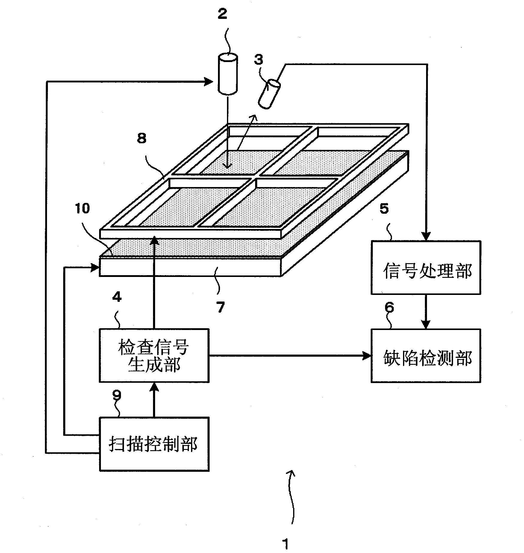
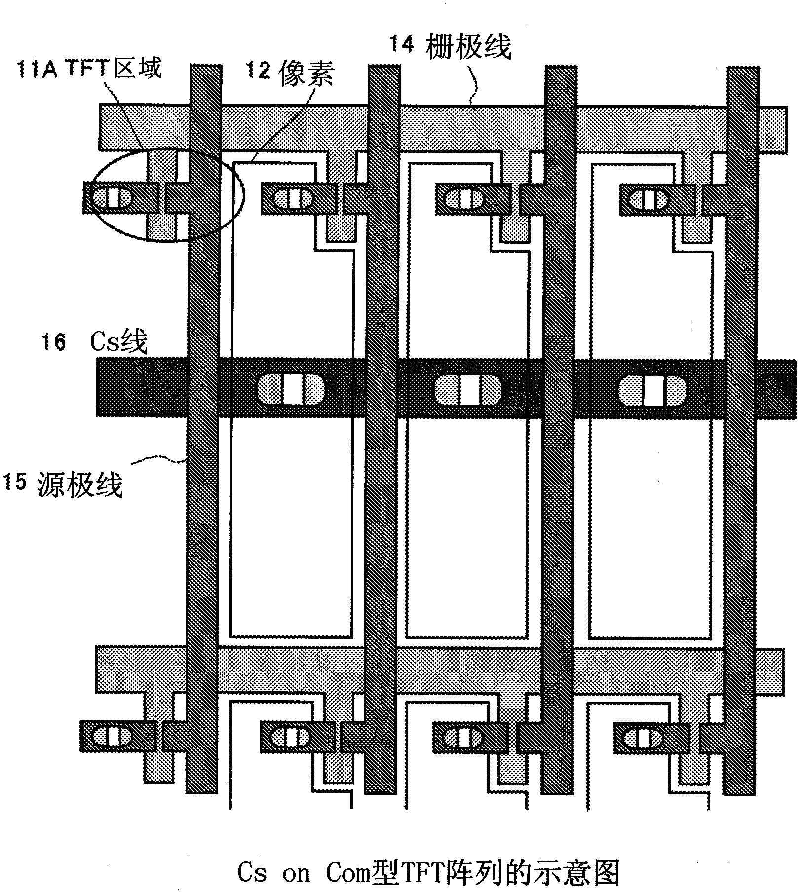
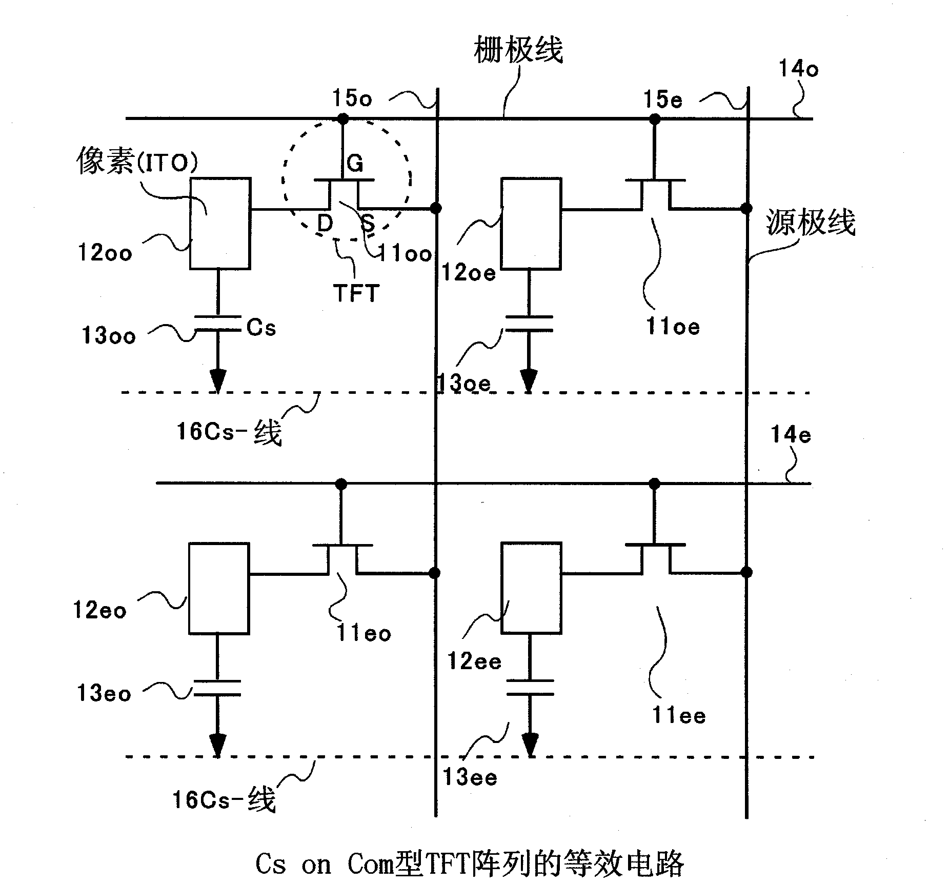
[0080] Hereinafter, embodiments of the present invention will be described in detail with reference to the drawings. Next, use figure 1 A structural example of a TFT substrate inspection device of the present invention will be described, using Figure 7 to Figure 18 The inspection method of the TFT substrate of the present invention will be described. Figure 7 to Figure 9 It is a diagram for explaining a first inspection method in which one gate period is set as a positive voltage holding time in a Cs on Com type TFT array in which pixels are connected to a common line. Figure 10 to Figure 12 It is a diagram for explaining the second inspection method in which one gate period is set as a negative voltage holding time in a Cs on Com type TFT array in which pixels are connected to a common line. Figure 13 to Figure 15 It is a diagram for explaining a third inspection method in which one gate period is set as a positive voltage holding time in a Cs on Gate type TFT array in...


PUM


Abstract

The invention relates to a TFT array inspection method and a TFT array inspection apparatus. In a drive pattern for driving pixels, a voltage to be applied to the pixels in one gate period is either a positive voltage or a negative voltage, and a TFT array is driven using a drive pattern for maintaining either the positive voltage or the negative voltage for the pixels in one period. By using this drive pattern, in a voltage maintaining time in one period of the one gate period, either the positive voltage or the negative voltage is maintained. Thus, since a voltage maintaining time not contributing to fault detection is deleted, the influence of the voltage maintaining time not contributing to the fault detection on a detection pixel voltage is eliminated, and a fault detection rate can be improved.

Description

technical field [0001] The present invention relates to a TFT array inspection process performed in a manufacturing process of a liquid crystal substrate or the like, and particularly relates to TFT array driving when performing a TFT array inspection. Background technique [0002] In the manufacturing process of semiconductor substrates such as liquid crystal substrates and organic electroluminescence (Electro Luminescence) substrates on which TFT arrays are formed, the manufacturing process includes a TFT array inspection process in which defects in the TFT array are detected. examine. [0003] The TFT array is used, for example, as a switching element for selecting pixels (pixel electrodes) of a liquid crystal display device. In a substrate having a TFT array, for example, a plurality of gate lines functioning as scanning lines are arranged in parallel, and a plurality of source lines described as signal lines are arranged perpendicular to the gate lines. , a TFT (Thin ...

Claims


Application Information

Patent Timeline
Patent Type & Authority Applications(China)
IPC IPC(8): G01N23/225G01R31/26G02F1/13G02F1/133G02F1/1368G09F9/00H01L21/66H01L29/786
CPCG01R31/305G09G3/3648G09G3/006
Inventor 西原隆治
Owner SHIMADZU SEISAKUSHO CO LTD
Features
  • R&D
  • Intellectual Property
  • Life Sciences
  • Materials
  • Tech Scout
  • Unparalleled Data Quality
  • Higher Quality Content
  • 60% Fewer Hallucinations
Learn More