Circuit structure of printed circuit board
A technology of printed circuit board and circuit structure, applied in the direction of printed circuit components, etc., can solve problems such as difficult impedance control, achieve easy impedance and reduce abnormal impedance
- Summary
- Abstract
- Description
- Claims
- Application Information
AI Technical Summary
Problems solved by technology
Method used
Image

Examples
Embodiment
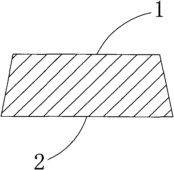
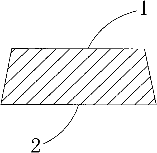
[0012] Embodiment: a circuit structure of a printed circuit board, the width of the upper surface 1 of the circuit is defined as the upper line width, the width of the lower surface 2 of the circuit is defined as the lower line width, and the difference between the lower line width and the upper line width is defined is a difference value, and the difference value is less than or equal to 0.0127mm (0.5mil). At design time, set the difference value to 0.5mil.
[0013] When the copper thickness of the line is 35 μm (1 oz), the average value of the difference is 0.0098044 mm (0.386 mil).
[0014] When the copper thickness of the line is 17.5 μm (0.5 oz), the average value of the difference is 0.0062992 mm (0.248 mil).
[0015] The circuit is an inner layer circuit of the printed circuit board.
PUM
 Abstract
Description
Claims
Application Information
 - R&D
- Intellectual Property
- Life Sciences
- Materials
- Tech Scout
- Unparalleled Data Quality
- Higher Quality Content
- 60% Fewer Hallucinations
Browse by: Latest US Patents, China's latest patents, Technical Efficacy Thesaurus, Application Domain, Technology Topic, Popular Technical Reports.
© 2025 PatSnap. All rights reserved.Legal|Privacy policy|Modern Slavery Act Transparency Statement|Sitemap|About US| Contact US: help@patsnap.com