Method for washing and purifying autologous oxide on surface of GaAs (gallium arsenide) and depositing Al2O3 medium

一种砷化镓、氧化物的技术,应用在使用液体的清洁方法、清洁方法和用具、化学仪器和方法等方向,能够解决栅极泄漏电流上升、栅极泄漏电流增加、器件性能退化等问题

Inactive Publication Date: 2012-02-01
FUDAN UNIV
View PDF3 Cites 4 Cited by
  • Summary
  • Abstract
  • Description
  • Claims
  • Application Information

AI Technical Summary

Problems solved by technology

The gate leakage current caused by the quantum tunneling effect increases exponentially as the thickness of the gate oxide layer decreases. When the thickness of the gate oxide layer is less than 2nm, the quantum tunneling effect causes a rapid increase in the gate leakage current, which eventually leads to a decrease in device performance. the degradation of

Method used


Image

  • Method for washing and purifying autologous oxide on surface of GaAs (gallium arsenide) and depositing Al2O3 medium
  • Method for washing and purifying autologous oxide on surface of GaAs (gallium arsenide) and depositing Al2O3 medium
  • Method for washing and purifying autologous oxide on surface of GaAs (gallium arsenide) and depositing Al2O3 medium

Examples


Embodiment 1

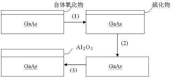
[0051] In the experiment, Si-doped n-type (100) oriented GaAs samples were used, and the doping concentration was about 1.0×10 17 cm -3 . After the GaAs sample was cleaved into small pieces, it was placed in trichlorethylene, acetone, alcohol and deionized water for 5 minutes for ultrasonic cleaning to remove surface grease and organic matter. Then put the GaAs sample in a dilute HF solution with a concentration of 2%, rinse the excess HF solution with deionized water after cleaning for 2 minutes, this step is to clean the oxides on the surface of GaAs. Then soak in 10% ammonia water for 5 minutes, and use the alkali to react with the GaAs autogenous oxide to remove it. In addition, this step can also neutralize the previous HF solution.

[0052] With 2g of CH 3 CSNH 2 , 4ml of absolute ethanol and 1ml of ammonia water to prepare a mixed solution, take out the GaAs sample with clean tweezers, and immediately put it into the mixed solution for passivation for 10 minutes, re...


PUM


Abstract

The invention belongs to the technical field of semiconductor materials, and in particular relates to a method for washing and purifying an autologous oxide on the surface of GaAs (gallium arsenide) and depositing an Al2O3 medium. The method comprises the following steps of: reacting a novel sulfur passivation agent with the autologous oxide on the GaAs surface for washing to generate a sulfide passivation film for isolating the GaAs and outside, thereby preventing reoxidation of the GaAs; by utilizing a pretreatment reaction between a reaction source trimethyl aluminum for Al2O3 deposition by using ALD (Atomic Layer Deposition) and the GaAs surface, further washing residual autologous oxide, sulfide and the like on the GaAs surface, and depositing the high-quality Al2O3 medium as a grid medium by adopting ALD, so that the GaAs and the outside environment are well isolated by the Al2O3 medium layer. The method disclosed by the invention has the advantages of simple process, favorable effect and provides a precondition for preparation of a GaAs device.

Description

technical field [0001] The invention belongs to the technical field of semiconductor materials, in particular to the cleaning and further deposition of Al on the surface of gallium arsenide 2 o 3 medium method. Background technique [0002] With the rapid development of the microelectronics industry and the optoelectronics industry, the demand for semiconductor lasers, optical fiber communication optical receiving components, and high-speed and high-frequency semiconductor devices made of GaAs and other III-V compound semiconductor materials is increasing. Therefore, GaAs and other III -The study of group V compound semiconductor materials has always been the focus of academia and industry. GaAs intrinsic materials are widely used in high-speed devices and high-temperature environments due to their high electron mobility, large band gap (1.43eV) and low carrier concentration. GaAs is considered to be very likely to replace silicon (Si) as the channel material of CMOS de...

Claims


Application Information

Patent Timeline
Patent Type & Authority Applications(China)
IPC IPC(8): H01L21/67H01L21/316B08B3/08
CPCH01L21/67H01L21/02178B08B3/08H01L21/02301H01L21/0228H01L21/316H01L21/306H01L21/02312H01L21/02052
Inventor 孙清清房润辰杨雯王鹏飞张卫
Owner FUDAN UNIV
Why Eureka
Try Eureka