Manufacturing method for silicon-on-insulator (SOI) structure provided with stepped oxidization buried layer

A fabrication method and technology of buried oxide layer, applied in semiconductor/solid-state device manufacturing, electrical components, circuits, etc., can solve problems such as short channels, and achieve the effects of reducing leakage current, reducing leakage current, and improving performance

Active Publication Date: 2015-02-04
SHANGHAI HUAHONG GRACE SEMICON MFG CORP
View PDF6 Cites 0 Cited by
  • Summary
  • Abstract
  • Description
  • Claims
  • Application Information

AI Technical Summary

Problems solved by technology

[0006] The problem to be solved by the present invention is to propose a new method for fabricating an SOI structure with a stepped oxide buried layer, so as to solve the short channel effect in the existing SOI structure

Method used


Image

  • Manufacturing method for silicon-on-insulator (SOI) structure provided with stepped oxidization buried layer
  • Manufacturing method for silicon-on-insulator (SOI) structure provided with stepped oxidization buried layer
  • Manufacturing method for silicon-on-insulator (SOI) structure provided with stepped oxidization buried layer

Examples


no. 1 example

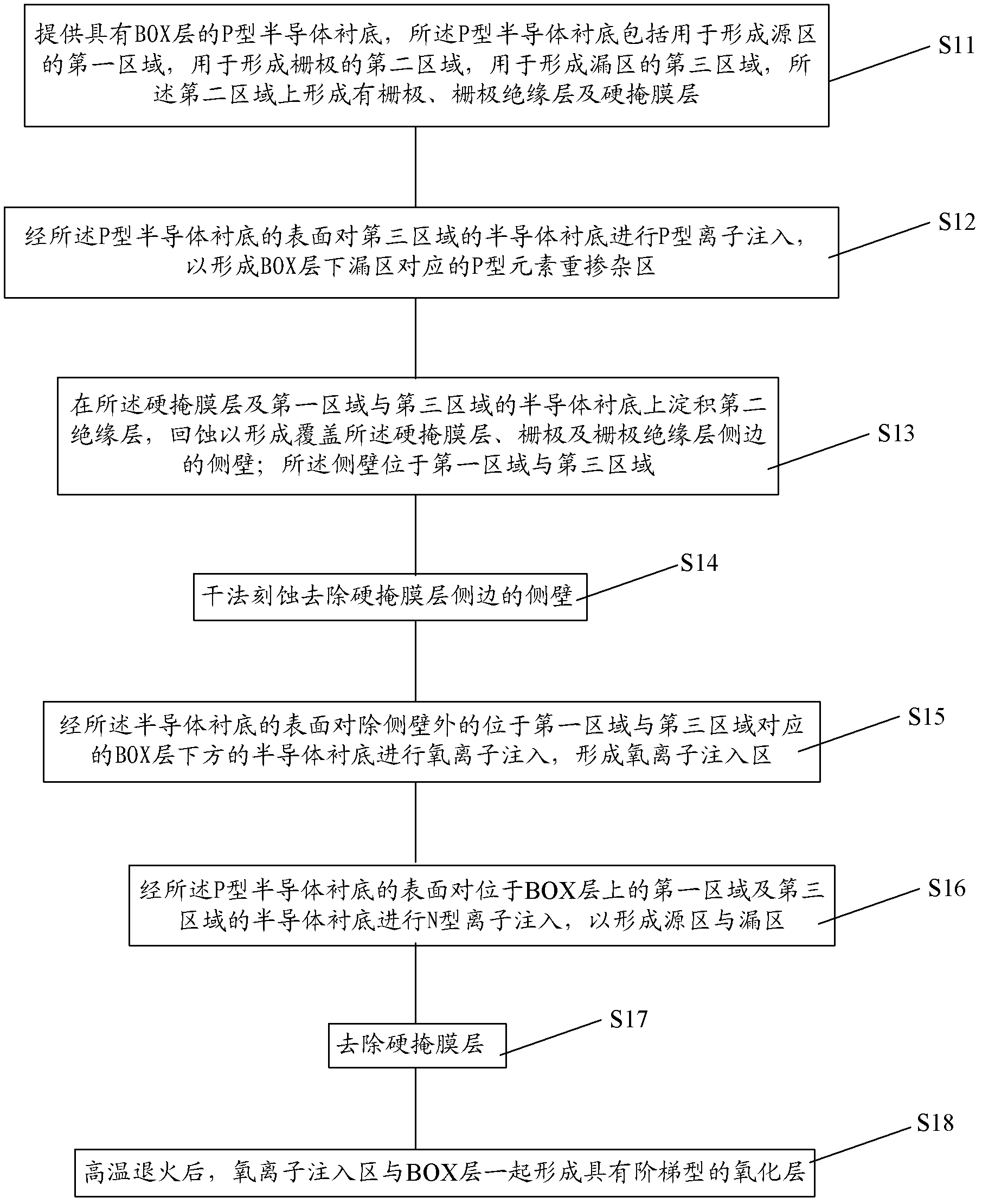
[0076] The present invention provides two methods for manufacturing SOI structures with stepped oxide buried layers. The first method is as follows: image 3 shown. The following combination Figure 4-Figure 17 This method will be specifically described.

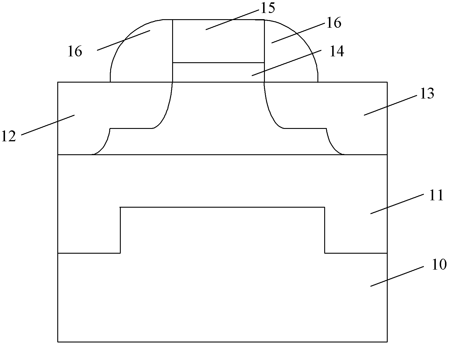
[0077] Step S11 is executed to provide a P-type semiconductor substrate having a BOX layer, the P-type semiconductor substrate comprising a first region for forming a source region, a second region for forming a gate, and a first region for forming a drain region. The third region, a gate, a gate insulating layer and a hard mask layer are formed on the second region.

[0078] In the specific implementation process of this step, the following steps S111-S114 are included.

[0079] Step S111, providing a P-type semiconductor substrate 20 with a structure such as Figure 4 As shown, the semiconductor substrate 20 includes a first region (not marked) for forming a source region, a second region (not marked) for forming a gat...

no. 2 example

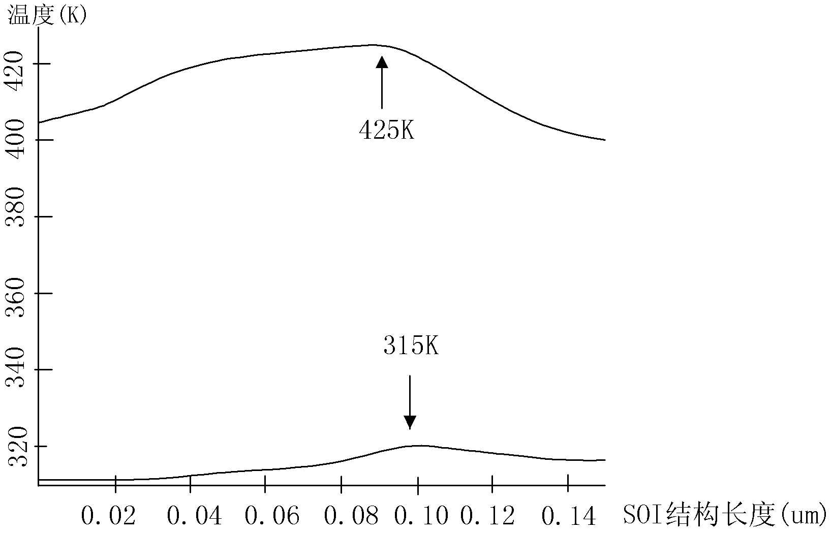
[0110] If the SOI structure provided by the first embodiment is called NMOS, the difference from the first embodiment is that the SOI structure provided by the second embodiment is PMOS. It can be understood that, regardless of NMOS or PMOS, the P-type element heavily doped region They are all regions with the lowest potential. Therefore, setting a P-type element heavily doped region in the PMOS SOI structure can also prevent the electric field lines drawn from the drain region in the existing DSBO SOI structure from partially terminating in the source region, and thus As a result, the height of the barrier at the end of the source region is reduced, which in turn leads to the problem that electrons in the source region easily cross the barrier and enter the drain region, which increases the threshold voltage of the SOI structure, reduces the leakage current when the SOI structure is in the off state, and improves the Performance of SOI structure devices.

[0111] The second m...


PUM


Abstract

The invention provides two methods for forming a silicon-on-insulator (SOI) structure provided with a stepped oxidization buried layer. The first method comprises the following steps of: providing a first region and a third region used for forming a source region and a drain region respectively, and a P-type semiconductor substrate of a second region on which a grid electrode, a grid electrode insulating layer and a hard mask layer are formed, wherein a BOX layer is arranged in the substrate, and a P-type element heavily-doped region corresponding the drain region is formed below the BOX layer; forming a side wall for covering the hard mask layer, the grid electrode and the grid electrode insulating layer; forming an N-type source region and an N-type drain region; performing oxygen ion implantation on the substrate positioned below the BOX layer corresponding to the source region and the drain region except the side wall; and performing high-temperature annealing to form an oxygen ion implantation region and the BOX layer into a stepped oxidization layer. The other method comprises the following steps of: forming an N-type doped region on the top layer of the substrate; and forming the source region and the drain layer in the doped region. Due to the adoption of the technical scheme provided by the invention, the short-channel effect of an existing SIO structure can be avoided.

Description

technical field [0001] The present invention relates to the field of semiconductor manufacturing, in particular to a method for manufacturing an SOI structure with a stepped oxide buried layer. Background technique [0002] In SOI (silicon-on-insulator) materials, because there is an insulating buried layer (usually a silicon dioxide buried layer, referred to as a buried oxide layer) between the top silicon film and the substrate silicon, SOI technology has many advantages beyond traditional bulk silicon. Technical advantages, such as: Compared with traditional bulk silicon CMOS, CMOS manufactured using SOI materials has the characteristics of high speed, low power consumption, and small source-drain parasitic capacitance, while avoiding the latch-up effect in bulk silicon CMOS. [0003] figure 1 Shown is an SOI structure with a buried oxide layer in the prior art, which includes: a semiconductor substrate 10, a gate insulating layer 14 and a gate 15 formed on the substrate...

Claims


Application Information

Patent Timeline
Patent Type & Authority Patents(China)
IPC IPC(8): H01L21/762
Inventor 苟鸿雁唐树澍
Owner SHANGHAI HUAHONG GRACE SEMICON MFG CORP
Why Eureka
Try Eureka